Pll circuit for reducing reference leak and phase noise

a reference leakage and phase noise technology, applied in the direction of electrical equipment, pulse automatic control, etc., can solve the problems of phase compared frequency, and achieve the effect of suppressing thermal noise, shortening the time required, and reducing spurious and noise amoun

Inactive Publication Date: 2011-11-24
PANASONIC CORP
View PDF2 Cites 11 Cited by
  • Summary
  • Abstract
  • Description
  • Claims
  • Application Information

AI Technical Summary

Benefits of technology

[0022]The present invention has been developed under the circumstances, and an object of the present invention is to provide a PLL circuit capable of reducing a reference leak and suppressing a phase noise.
[0038]As should be appreciated from the above, it is possible to shorten a lock time required after a power supply is ON or a reset state is released, and to reduce a spurious caused by a reference leak or a jitter in a lock state where the comparison signal is locked to the reference signal.

Problems solved by technology

As a consequence, in the configurations disclosed in the above illustrated publications, a spurious (reference leak) results in the frequencies with which the phases are compared.

Method used


Image

  • Pll circuit for reducing reference leak and phase noise
  • Pll circuit for reducing reference leak and phase noise
  • Pll circuit for reducing reference leak and phase noise

Examples


embodiment 1

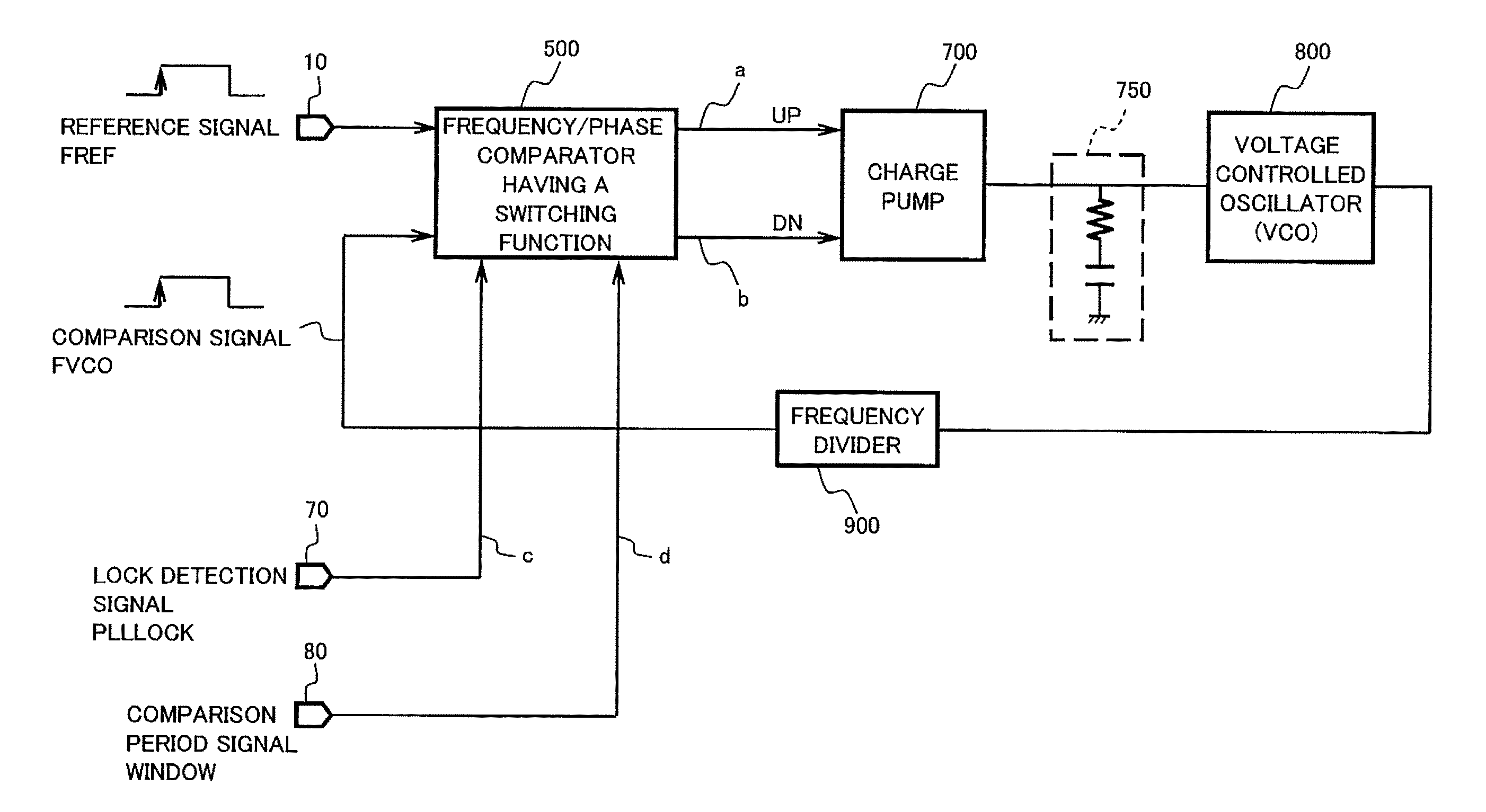
[0060]FIG. 1 shows a configuration of a PLL circuit according to Embodiment 1 of the present invention. The PLL circuit includes a frequency / phase comparator 500 having a switching function (hereinafter simply referred to as frequency / phase comparator 500), a charge pump 700, a loop filter 750, a voltage controlled oscillator (VCO) 800 and a frequency divider 900 for dividing a frequency of an output of the VCO 800.

[0061]An oscillating frequency of the VCO 800 is controlled in accordance with a voltage of the loop filter 750. A capacitor in the loop filter 750 is charged or discharged by an output current of the charge pump 700, and a voltage of the capacitor changes according to the charging or discharging. The charge pump 700 is fed with phase error output signals (UP signal and DN signal) output from the frequency / phase comparator 500, and outputs a current according to the phase error output signals. The frequency / phase comparator 500 is fed with a reference signal FREF10 and a ...

embodiment 2

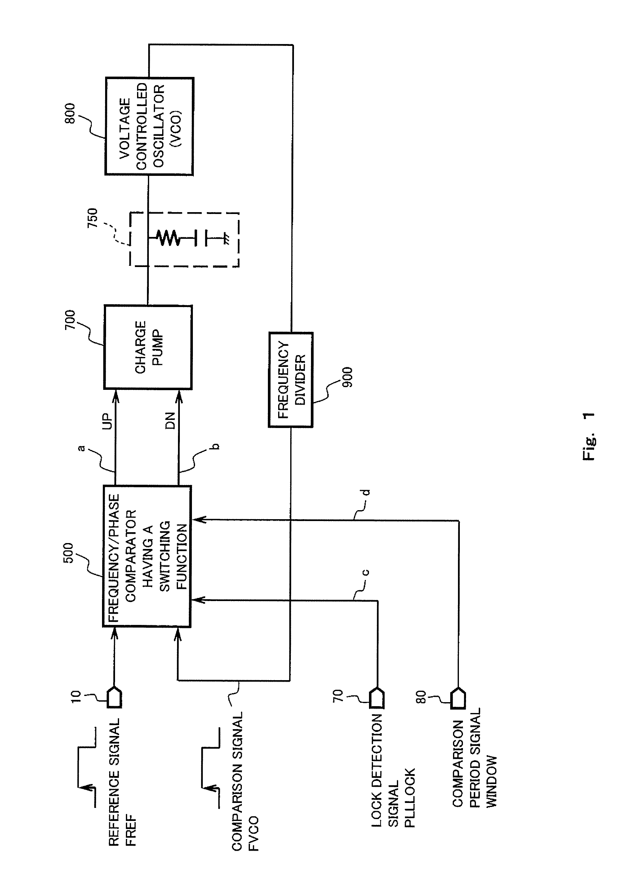
[0095]FIG. 2 is a view showing an exemplary configuration of a PLL circuit according to Embodiment 2 of the present invention. In this embodiment, the same components and constituents as those in Embodiment 1 are designated by the same reference symbols and will not be described. In this embodiment, the PLL circuit includes a frequency / phase comparator 550 having a switching unit which is provided with a reset input terminal, instead of the frequency / phase comparator 500 having a switching function of Embodiment 1.

[0096]FIG. 5 is a view showing an internal configuration of the frequency / phase comparator 550 having a switching function in the PLL circuit of FIG. 2. Referring to FIG. 5, in this embodiment, the frequency / phase comparator 550 is configured such that a reset signal NRST60 is input to a frequency comparator circuit 350. FIG. 14 shows an internal configuration of the frequency comparator circuit 350 shown in FIG. 5.

[0097]The frequency comparator circuit 350 includes a freq...

embodiment 3

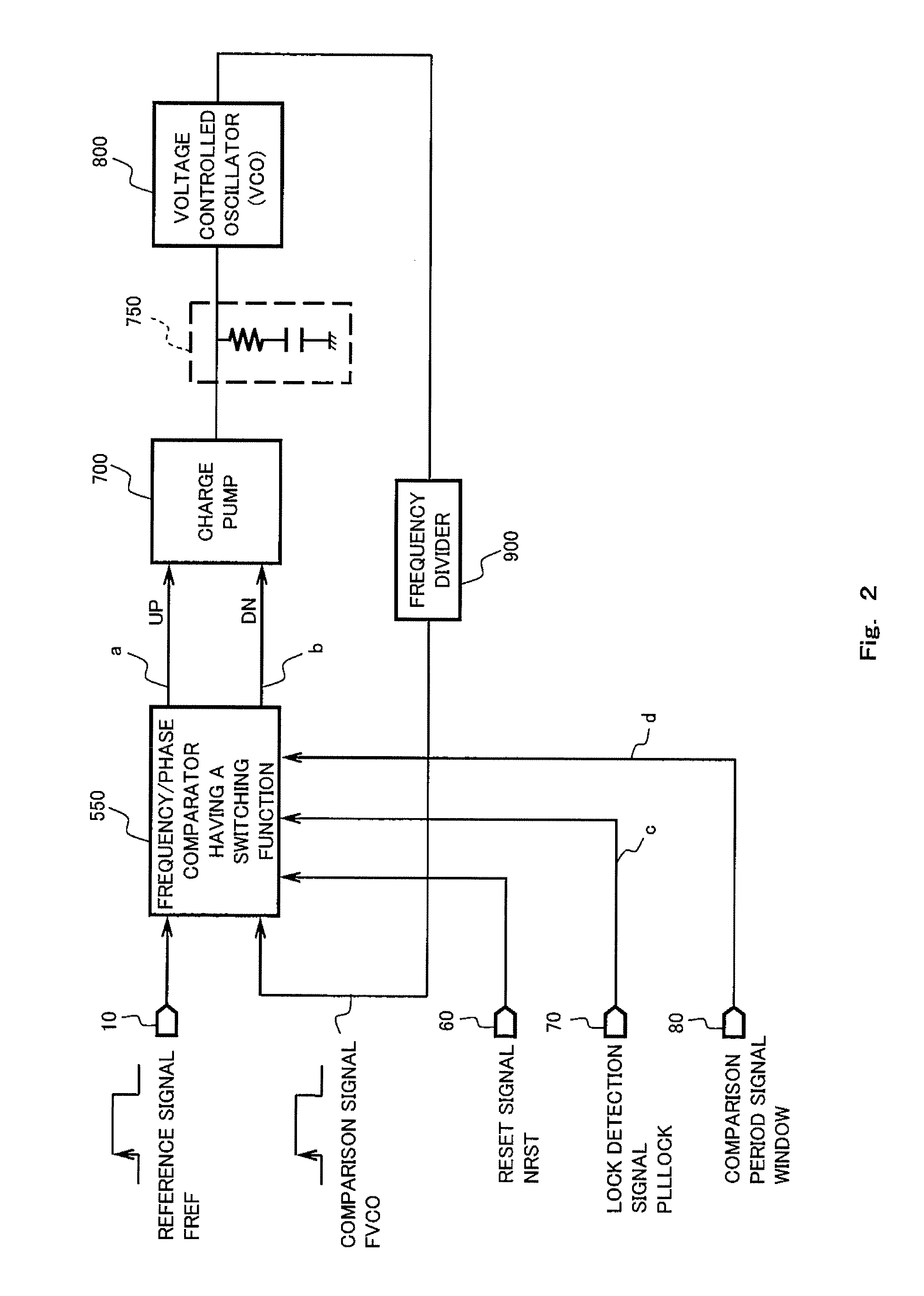
[0104]FIG. 3 is a view showing an exemplary configuration of a PLL circuit according to Embodiment 3 of the present invention. In this embodiment, the same components and constituents as those in Embodiment 2 are designated by the same reference symbols and will not be described.

[0105]The PLL circuit of Embodiment 3 is different from the PLL circuit of Embodiment 2 in that a frequency / phase comparator 555 having a switching function includes a lock detection signal generating unit 600 for generating the lock detection signal PLLLOCK70, according to the comparison period signal WINDOW80 and the reference signal FREF10.

[0106]FIG. 6 is a view showing an internal configuration of the frequency / phase comparator 555 having a switching function in the PLL circuit of FIG. 3. Referring to FIG. 6, the lock detection signal generating unit 600 is fed with the comparison period signal WINDOW80 as a data signal and the reference signal FREF10 as a clock signal.

[0107]The lock detection signal gen...


PUM


Abstract

A phase locked loop circuit comprises a charge pump fed with a phase error output signal; a loop filter charged or discharged with an output of the charge pump; an oscillator, an oscillating frequency of which is controlled by a voltage of the loop filter; and a frequency / phase comparator having a switching function which is fed with a reference signal and an output signal of the oscillator and outputs the phase error output signal; the frequency / phase comparator being configured to, based on a lock detection signal, switch between comparing frequencies by detecting rising edges of the reference signal and the comparison signal to detect a phase difference between the reference signal and the comparison signal, and comparing phases by detecting voltage levels of the reference signal and the comparison signal to detect a phase difference between the reference signal and the comparison signal.

Description

[0001]The disclosure of Japanese Patent Application No. 2010-118010 filed on May 24, 2010 and No. 2011-12793 filed on Jan. 25, 2011 including specification, drawings and claims are incorporated herein by reference in its entirety.BACKGROUND OF THE INVENTION[0002]1. Field of the Invention[0003]The present invention relates to a clock generating circuit such as a PLL (phase locked loop) circuit. Particularly, the present invention relates to a technique for controlling a frequency / phase comparator according to an operational state of the PLL circuit.[0004]2. Description of the Related Art[0005]FIG. 16 shows a frequency / phase comparator 300 which is a constituent in the conventional PLL circuit disclosed in Japanese Laid-Open Patent Application Publication No. Hei. 11-234123.[0006]Referring to FIG. 16, a reference signal FREF and a comparison signal FVCO are input to input terminals 10 and 20, respectively, and are input to an edge comparator 50 through inverters 1 and 2, respectively....

Claims


Application Information

Patent Timeline
Patent Type & Authority Applications(United States)
IPC IPC(8): H03L7/06
CPCH03L7/087
Inventor KINUGASA, NORIHIDECHIBA, KOJI
Owner PANASONIC CORP
Why Eureka
Try Eureka