3D two-bit-per-cell NAND flash memory

a nand flash memory and two-bit technology, applied in semiconductor devices, digital storage, instruments, etc., can solve the problem of limiting the number of cells that can be implemented using vertical nand string structures

Active Publication Date: 2011-11-24
MACRONIX INT CO LTD
View PDF5 Cites 296 Cited by
  • Summary
  • Abstract
  • Description
  • Claims
  • Application Information

AI Technical Summary

Benefits of technology

[0013]Methods for manufacturing a 3D array of memory cells including bottom and top memory cubes and a source plane between the...

Problems solved by technology

However, there is a limit on the number of layers of cells that can be implemented using vertical NAN...

Method used


Image

  • 3D two-bit-per-cell NAND flash memory
  • 3D two-bit-per-cell NAND flash memory
  • 3D two-bit-per-cell NAND flash memory

Examples


Embodiment Construction

[0026]A detailed description of embodiments of the present invention is provided with reference to the FIGS. 1-19.

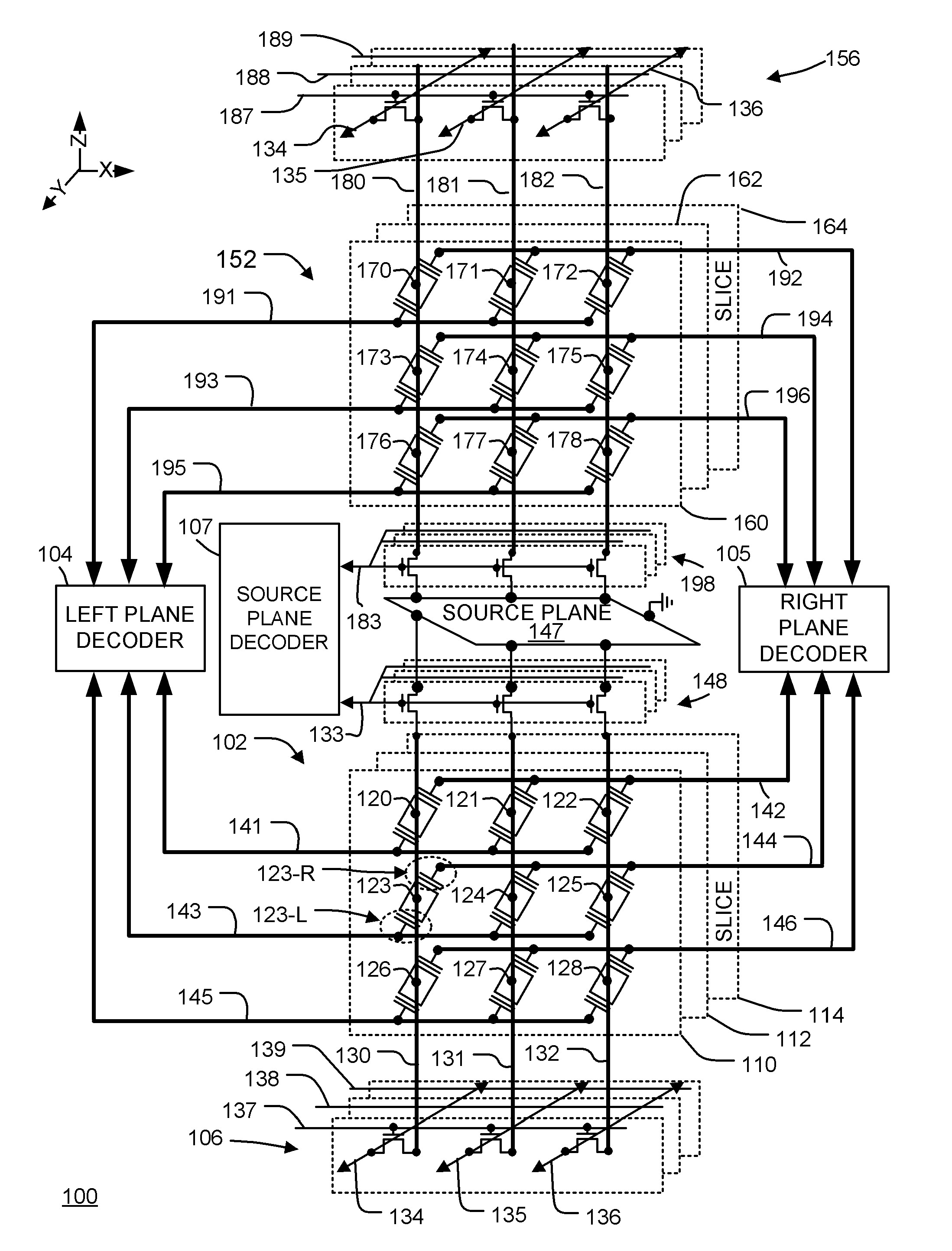
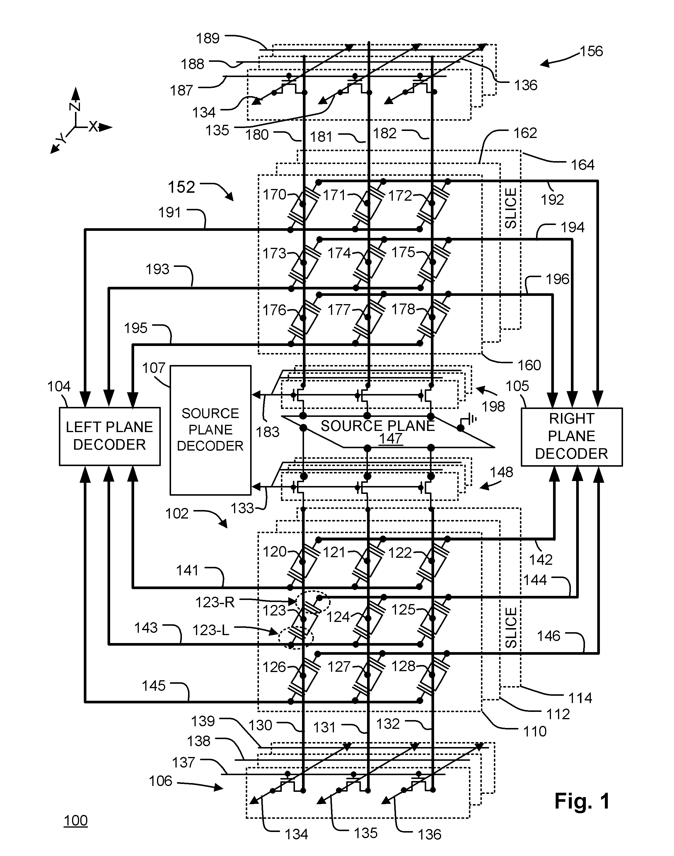
[0027]FIG. 1 is a schematic diagram of a 3D memory device 100 including a common source plane 147 arranged between a bottom memory cube 102 of memory cells and a top memory cube 152 of memory cells.

[0028]The schematic diagram of FIG. 1 shows “slices”110, 112, 114 which lie in X-Z planes of the bottom memory cube 102. In the illustrated schematic, there are nine two-cell unit structures 120-128 in slice 110, each two-cell unit structure 120-128 having two memory cells including having separate charge storage structures and left and right gates. Embodiments can include many two-cell unit structures per slice.

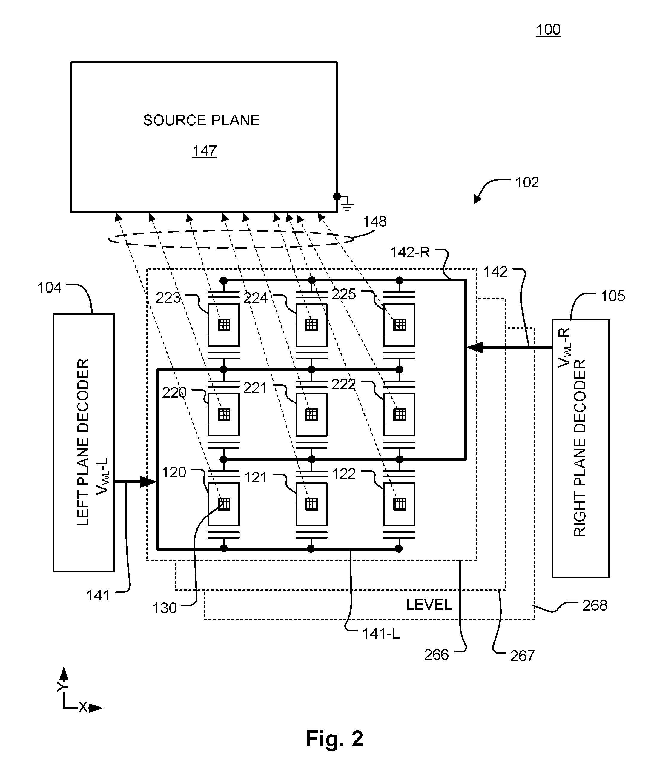
[0029]The bottom memory cube 102 includes an array of memory cells arranged for NAND-type decoding, using a left plane decoder 104, right plane decoder 105, a bottom set of pillar select transistors 106, and source plane decoder 107. The left and right side memory cell...


PUM


Abstract

A 3D memory device is described which includes bottom and top memory cubes having respective arrays of vertical NAND string structures. A common source plane comprising a layer of conductive material is between the top and bottom memory cubes. The source plane is supplied a bias voltage such as ground, and is selectively coupled to an end of the vertical NAND string structures of the bottom and top memory cubes. Memory cells in a particular memory cube are read using current through the particular vertical NAND string between the source plane and a corresponding bit line coupled to another end of the particular vertical NAND string.

Description

BACKGROUND OF THE INVENTION[0001]1. Field of the Invention[0002]The present invention relates to high density memory devices, and particularly to memory devices in which multiple planes of memory cells are arranged to provide a three-dimensional 3D array.[0003]2. Description of Related Art[0004]As critical dimensions of devices in integrated circuits shrink to the limits of common memory cell technologies, designers have been looking to techniques for stacking multiple planes of memory cells to achieve greater storage capacity, and to achieve lower costs per bit. For example, thin film transistor techniques are applied to charge trapping memory technologies in Lai, et al., “A Multi-Layer Stackable Thin-Film Transistor (TFT) NAND-Type Flash Memory”, IEEE Int'l Electron Devices Meeting, 11-13 Dec. 2006; and in Jung et al., “Three Dimensionally Stacked NAND Flash Memory Technology Using Stacking Single Crystal Si Layers on ILD and TANOS Structure for Beyond 30 nm Node”, IEEE Int'l Elec...

Claims


Application Information

Patent Timeline
IPC IPC(8): G11C16/04H01L21/336
CPCG11C16/0483H01L27/11578H01L29/7926H01L29/66833H01L27/11582H10B43/20H10B43/27
Inventor LUNG, HSIANG-LANLUE, HANG-TINGSHIH, YEN-HAOLAI, ERH-KUNLEE, MING HSIUWANG, TIEN-YEN
Owner MACRONIX INT CO LTD
Why Eureka
Try Eureka