CMOS three-dimensional image sensor detectors having reduced inter-gate capacitance, and enhanced modulation contrast

a three-dimensional image sensor and detector technology, applied in the field of three-dimensional image sensor detectors having reduced inter-gate capacitance and enhanced modulation contrast, can solve the problem of inter-gate capacitance decreasing, and achieve the effect of reducing inter-gate capacitan

Active Publication Date: 2011-12-01
MICROSOFT TECH LICENSING LLC
View PDF1 Cites 64 Cited by
  • Summary
  • Abstract
  • Description
  • Claims
  • Application Information

AI Technical Summary

Benefits of technology

[0028]The present invention proves three-dimensional CMOS sensors in which adjacent gates need not be in close proximity to function. As distance between adjacent gates increases, inter-gate capacitance decreases, as do mal-effects of such capacitance upon detection power consumption. Embodiments of the present invention eliminate the barrier regions implanted between adjacent elongated finger-like gates, as described in the '454 patent. Instead, elongated finger-like p+ regions are implanted beneath the gates, preferably before the polysilicon gates are created. Alternatively, elongated finger-like p+ regions are implanted adjacent but slightly overlapping the edges of the gates, preferably after the polysilicon gates are formed. If desired, both p+ region types may be used simultaneously.

Problems solved by technology

As distance between adjacent gates increases, inter-gate capacitance decreases, as do mal-effects of such capacitance upon detection power consumption.

Method used


Image

  • CMOS three-dimensional image sensor detectors having reduced inter-gate capacitance, and enhanced modulation contrast
  • CMOS three-dimensional image sensor detectors having reduced inter-gate capacitance, and enhanced modulation contrast
  • CMOS three-dimensional image sensor detectors having reduced inter-gate capacitance, and enhanced modulation contrast

Examples


Embodiment Construction

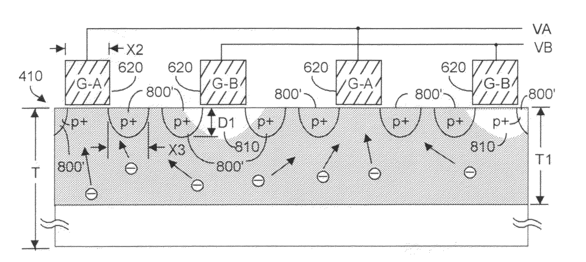
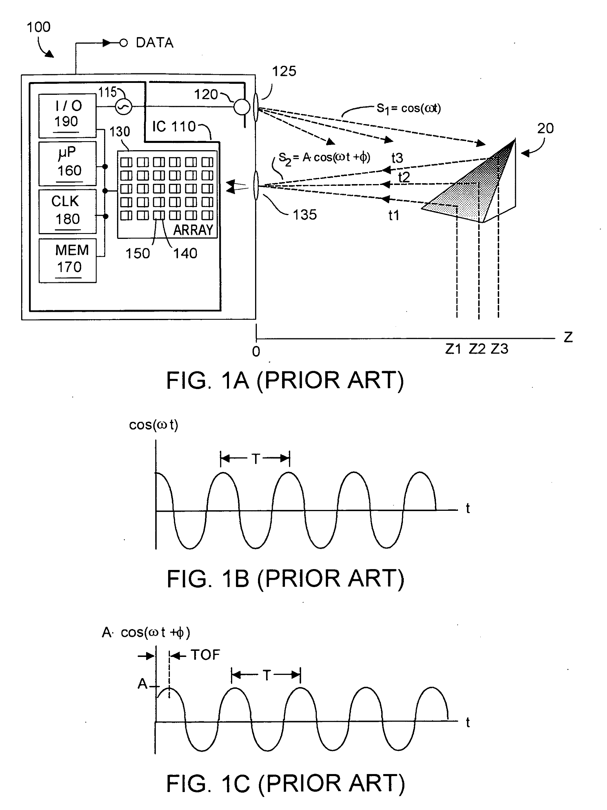
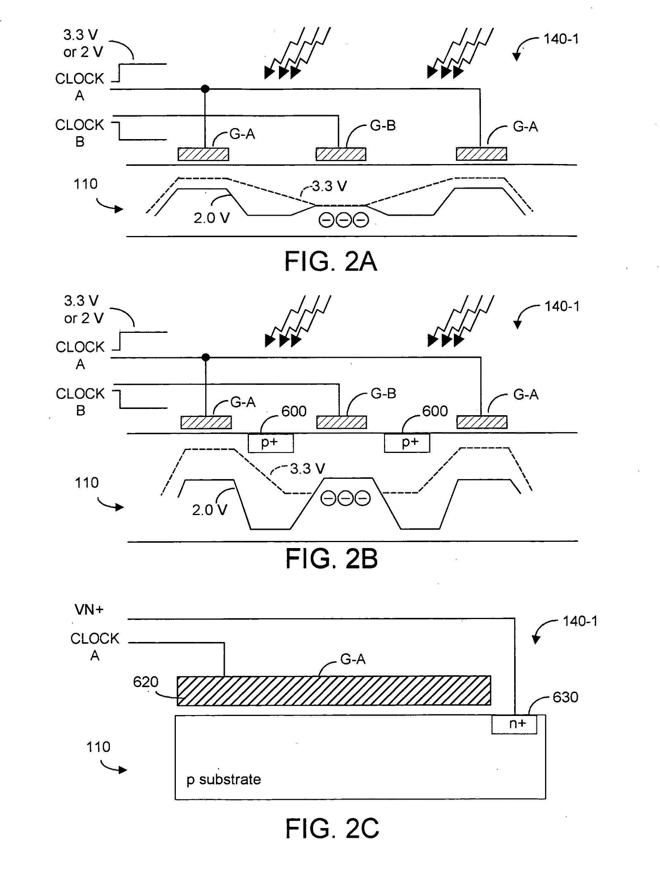
[0043]Embodiments of the present invention may be practiced with phase-based TOF systems such as depicted in FIG. 1A as exemplified by numerous U.S. patents to Canesta, Inc., include U.S. Pat. No. 7,352,454 (2008) or with non-phase based systems, e.g., as described in U.S. Pat. No. 6,323,942 (2001), assigned to Canesta, Inc. Embodiments, of the present invention to improve collection of photocharge whose creation time is known, and to impede collection of photocharge whose creation time is not known (i.e., late arriving charge) can be implemented by modifying the structure of sensors 140 in FIG. 1A. Of course the present invention may be used with other sensors and may be used in non-TOF applications.

[0044]Sensors as described with respect to FIG. 1A, modeled on the '454 patent, thus are a good starting point. To recapitulate the description of the '454 sensors, the sensor structures included finger-shaped gate structures that extended along a y-axis, and were spaced-apart from each...


PUM


Abstract

A CMOS detector with pairs of interdigitated elongated finger-like collection gates includes p+ implanted regions that create charge barrier regions that can intentionally be overcome. These regions steer charge to a desired collection gate pair for collection. The p+ implanted regions may be formed before and / or after formation of the collection gates. These regions form charge barrier regions when an associated collection gate is biased low. The barriers are overcome when an associated collection gate is high. These barrier regions steer substantially all charge to collection gates that are biased high, enhancing modulation contrast. Advantageously, the resultant structure has reduced power requirements in that inter-gate capacitance is reduced in that inter-gate spacing can be increased over prior art gate spacing and lower swing voltages may be used. Also higher modulation contrast is achieved in that the charge collection area of the low gate(s) is significantly reduced.

Description

CROSS-REFERENCE TO CO-PENDING APPLICATION[0001]Priority is claimed from applicants' U.S. provisional patent application Ser. No. 61 / 207,913, filed 17 Feb. 2009, and assigned to Canesta, Inc., of Sunnyvale, Calif., assignee herein.BACKGROUND OF THE INVENTION[0002]The invention relates generally to CMOS-implementable image sensors suitable for three-dimensional applications including time-of-flight (TOF) and phase-based TOF range or depth systems. More specifically, the invention is directed to reducing inter-gate capacitance in such sensors, and enhancing modulation contrast.[0003]It is useful at this juncture to briefly describe TOF systems that can benefit from the present invention. FIGS. 1A-1C depict a phase-based TOF system 100 such as described in U.S. Pat. No. 7,352,454 (2008) entitled Methods and Systems for Improved Charge Management for Three-Dimensional and Color Sensing. The '454 patent is assigned to Canesta, Inc. of Sunnyvale, Calif. and is incorporated herein by refere...

Claims


Application Information

Patent Timeline
Patent Type & Authority Applications(United States)
IPC IPC(8): G01C3/08G01B11/26H01L27/146G01S7/4861G01S7/4863G01S17/894
CPCG01S7/4863G01S17/89H01L27/14643G01J1/42H01L27/14605H01L27/14603H01L27/14614G01S17/894G01S7/4861
Inventor BAMJI, CYRUS
Owner MICROSOFT TECH LICENSING LLC
Why Eureka
Try Eureka