
Non-volatile memory device

a memory device and non-volatile technology, applied in the field of non-volatile memory devices, can solve the problems of unnecessarily increasing the voltage level of the selected word line wlb>2/b>, more serious problems, and faulty operation, so as to improve the discharge characteristics, improve the program and read characteristics, and prevent the voltage level of the bit line and the word line.

Active Publication Date: 2011-12-01
SK HYNIX INC
View PDF3 Cites 10 Cited by
  • Summary
  • Abstract
  • Description
  • Claims
  • Application Information

AI Technical Summary

Benefits of technology

The present invention provides a non-volatile memory device that solves problems associated with existing technologies. The device includes a cell array with multiple bit lines and word lines, a column switching unit to select a bit line, and a discharge unit to discharge non-selected bit lines during read or write operations. The device also includes a coding system to selectively control which bit line to discharge. The technical effects of the invention include improving the operation reliability, preventing voltage levels from increasing, improving program and read characteristics, and improving discharge characteristics.

Problems solved by technology

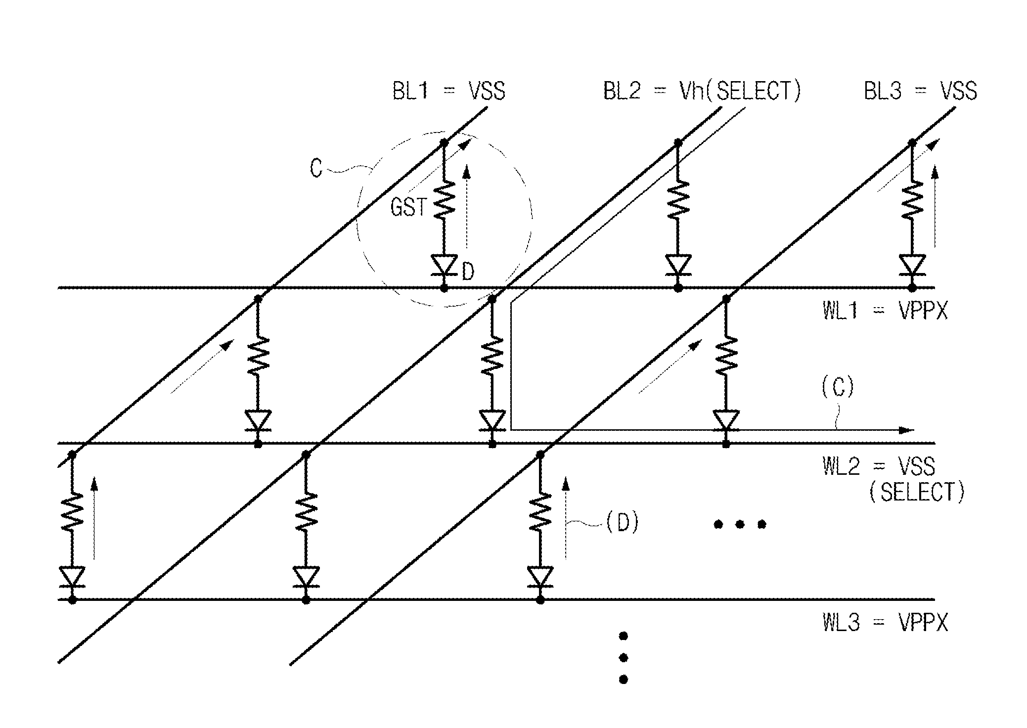
Therefore, a reverse leakage current flows in a diode of each non-selected cell, such that a voltage level of the selected word line WL2 is unnecessarily increased.
Specifically, in case of a structure in which the bit line BL shares two mats, a leakage current generated from two mats flows in the word line WL2, which may induce more serious problems.
Specifically, an unexpected current may flow through a non-selected bit line during an operation of the memory device having a relatively long sensing time, and the unexpected current may cause the faulty operation.
That is, a faulty operation may be caused by the leakage current generated in the operation of the memory device, and thus program and read properties and the operation reliability of the memory device may be decreased at step S5.

Method used


Image

  • Non-volatile memory device
  • Non-volatile memory device
  • Non-volatile memory device

Examples


Embodiment Construction

[0055]Reference will now be made in detail to the embodiments of the present invention, examples of which are illustrated in the accompanying drawings. Wherever possible, the same reference numbers will be used throughout the drawings to refer to the same or like parts.

[0056]FIG. 7 is a circuit diagram illustrating a non-volatile memory device according to an embodiment of the present invention.

[0057]Referring to FIG. 7, the non-volatile memory device includes a plurality of mats, a plurality of column switching units 100 and 110, and a plurality of discharge units 120 to 160. Each mat includes a unit cell C formed at an intersectional area between a bit line BL and a word line WL.

[0058]For convenience of description and better understanding of the present invention, the following embodiment of the present invention provides an exemplary structure in which a bit line BL is shared by two adjacent mats. As illustrated in FIG. 7, even-numbered bit lines BL0, BL2, BL4, BL6, BL8, BL10, B...


PUM


Abstract

A non-volatile memory device includes a plurality of mats, each of which includes a unit cell in an intersection area between each of a plurality of word lines and each of a plurality of bit lines such that a read or write operation of data is achieved in each mat, a column switching unit configured to select any one of bit lines from among the plurality of bit lines according to a column selection signal, and selectively control a connection between the selected bit line and a global bit line, and a discharge unit, in an active mode in which the read or write operation is achieved, configured to discharge the remaining bit lines other than the selected bit line from among the plurality of bit lines in response to a bit line discharge signal.

Description

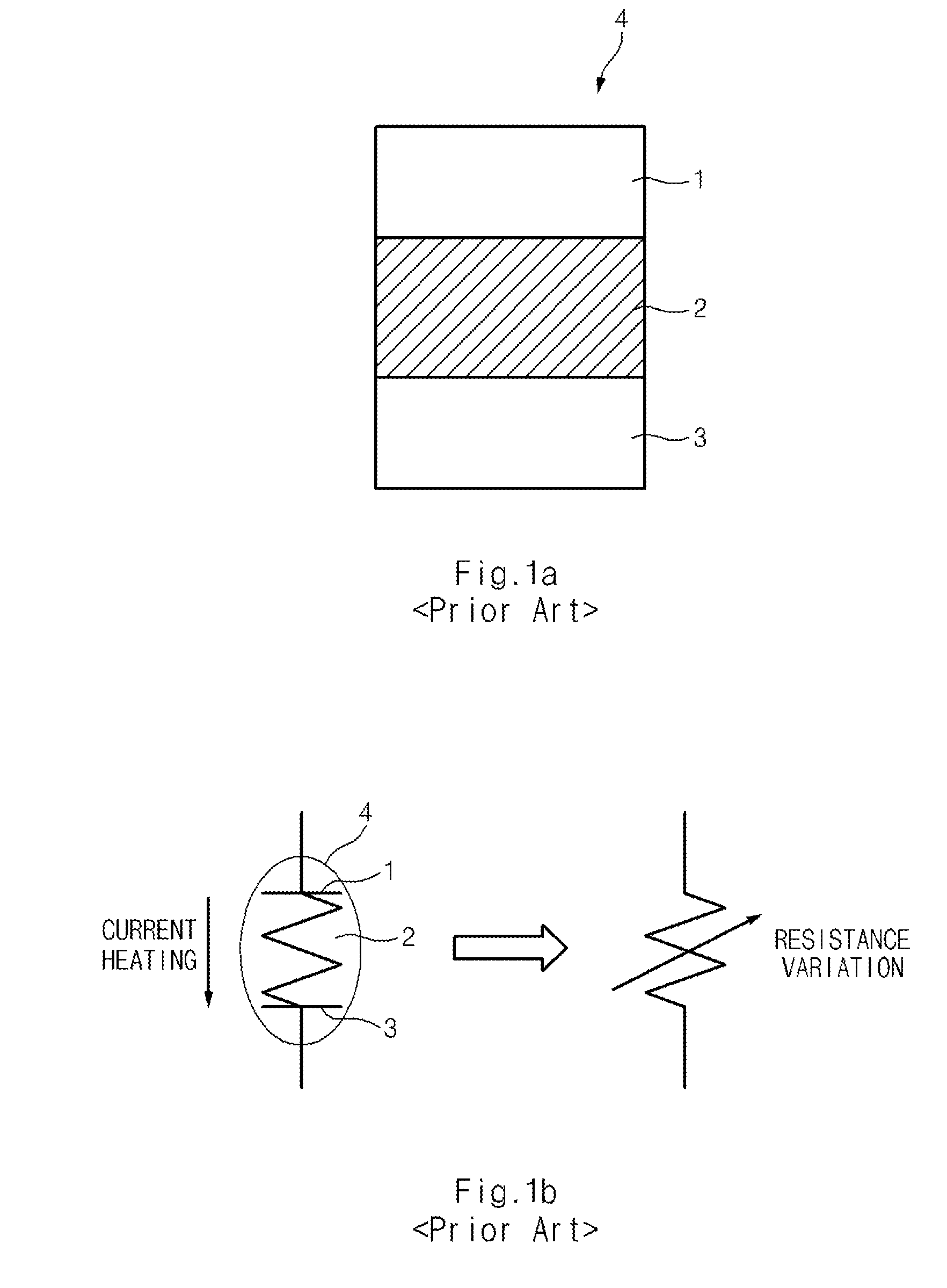
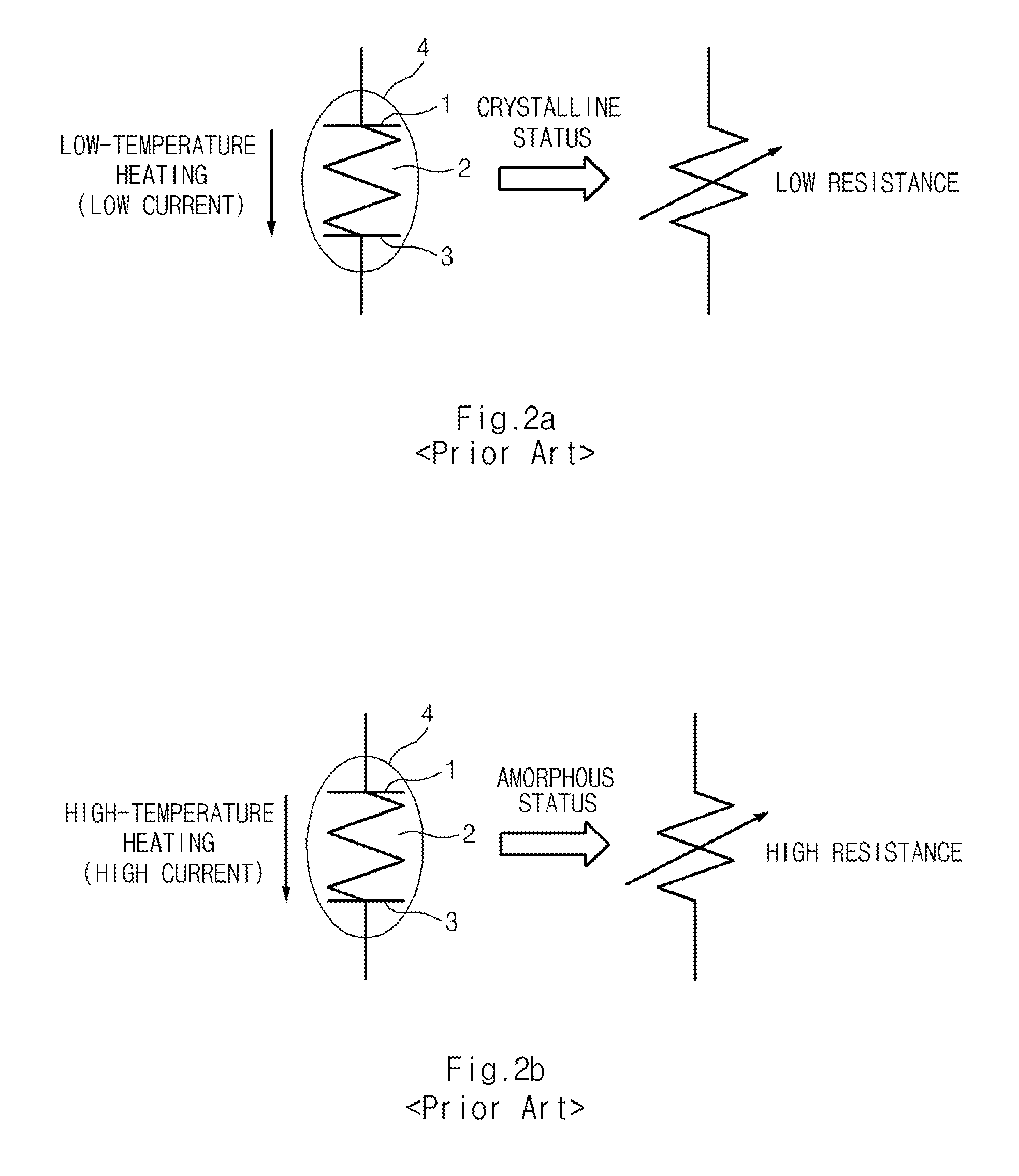
CROSS-REFERENCE TO RELATED APPLICATION[0001]The priority of Korean patent application No. 10-2010-0049654 filed on May 27, 2010, the disclosure of which is hereby incorporated in its entirety by reference, is claimed.BACKGROUND OF THE INVENTION[0002]Embodiments of the present invention relate to a non-volatile memory device, and more specifically, to a technology for increasing the operation reliability of the device.[0003]Memory devices may be classified into a volatile memory device and a non-volatile memory device. The non-volatile memory device includes a non-volatile memory cell capable of preserving stored data even when not powered. For example, the non-volatile memory device may be implemented as a flash random access memory (flash RAM), a phase change random access memory (PCRAM), or the like.[0004]The PCRAM includes a memory cell that is implemented using a phase change material such as germanium antimony tellurium (GST), wherein the GST changes to a crystalline phase or a...

Claims


Application Information

Patent Timeline
Patent Type & Authority Applications(United States)
IPC IPC(8): G11C7/00
CPCG11C7/12G11C2213/72G11C13/0004G11C5/063G11C13/004G11C13/0069G11C16/24
Inventor PARK, KYOUNG WOOK
Owner SK HYNIX INC
Learn More