User equipment for simultaneously transmitting signals to which different wireless communication systems are applied through a plurality of frequency bands

Active Publication Date: 2011-12-01
LG ELECTRONICS INC
8 Cites 52 Cited by

AI-Extracted Technical Summary

Problems solved by technology

In this case, since two antennas are designed for transmission and reception, respectively, in accordance with the related art, a problem occurs in that intermodulation distortion (IMD) occurs at the RF front e...

Benefits of technology

[0018]According to the embodiments of the present invention, the user equipment satisfies SAR condition when simultaneously transmitting signals, to which different w...

Abstract

A user equipment (UE) including first and second antennas; a first wireless communication chip configured to output first and second signals corresponding to first and second frequency bands, respectively; a second wireless communication chip configured to output thirds signals corresponding to a third frequency band; and a radio frequency (RF) front-end module configured to transmit the first and second signals corresponding to the first and second frequency bands output from the first wireless communication chip to the first antenna, transmit the third signal corresponding to the third frequency band output from the second wireless communication chip to the first antenna, transmit the second signal corresponding to the second frequency band externally received in the first antenna to the first wireless communication chip through a secondary Rx path, transmit the second signal corresponding to the second frequency band externally received in the second antenna to the first wireless communication chip through a primary Rx path, and transmit the third signal corresponding to the third frequency band received in the first and second antennas to the second wireless communication chip.

Application Domain

Technology Topic

Image

  • User equipment for simultaneously transmitting signals to which different wireless communication systems are applied through a plurality of frequency bands
  • User equipment for simultaneously transmitting signals to which different wireless communication systems are applied through a plurality of frequency bands
  • User equipment for simultaneously transmitting signals to which different wireless communication systems are applied through a plurality of frequency bands

Examples

  • Experimental program(2)

Example

First Embodiment
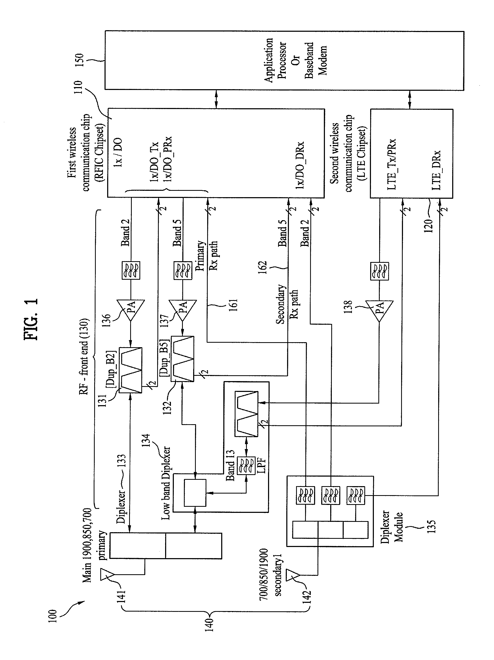
[0035]FIG. 1 is a diagram illustrating an example of a configuration of a user equipment 100 according to the first embodiment of the present invention. As shown in FIG. 1, the user equipment 100 includes a first wireless communication chip 110, a second wireless communication chip 120, an RF front-end module 130, an antenna 140, and an application processor or baseband modem 150.
[0036]In the embodiment in FIG. 1, the RF front-end module 130 includes duplexers 131 and 132, diplexers 133, 134 and 135, and power amplifiers 136, 137 and 138. The antenna 140 also includes a primary antenna 141 and one or more secondary antennas 142.
[0037]Further, a radio wave of a specific frequency band is used for wireless communication. The first and second wireless communication chips 110 and 120 modulate original signals (baseband signals) to high frequency band signals during signal transmission, and demodulate the received high frequency band signals to the baseband signals during signal reception. Each of the wireless communication chips 110 and 120 may be implemented as a “radio frequency (RF) chip” that modulates a signal processed at a baseband to a high frequency band signal, or may be implemented as an “RF and baseband chip” where a baseband chip that processes a baseband signal is combined with an RF chip that modulates a signal processed at a baseband to a high frequency band signal or demodulates the received signal to a low frequency band signal during signal transmission and reception to and from the baseband chip to process the modulated signal or the demodulated signal to the baseband signal.
[0038]As illustrated in FIG. 1, the user equipment 100 according to an embodiment of the present invention is implemented in such a manner that the first wireless communication chip 110 and the second wireless communication chip 120 are provided separately from the application processor or the baseband modem 150.
[0039]Also, although the first and second wireless communication chips 110 and 120 may be provided as separate chips as illustrated in FIG. 1, they may be provided as one chip.
[0040]As described above, the first wireless communication chip 110 and the second wireless communication chip 120 process the original signal to the high frequency band signal during signal transmission, whereas they process the high frequency band signal to the baseband signal. Also, the first wireless communication chip 110 and the second wireless communication chip 120 perform modulation/demodulation functions, respectively.
[0041]If the user equipment (UE) 100 needs to simultaneously transmit signals through the wireless communication chips 110 and 120 to which different wireless communication schemes are applied, the first wireless communication chip 110 processes the original signal to the first frequency band signal, and at the same time the second wireless communication chip 120 processes the original signal to the second frequency band signal. In other words, the user equipment 100 can transmit the signals by modulating the signals to different frequency band signals through the first and second wireless communication chips 110 and 120 during signal transmission. In general, when simultaneously transmitting the signals processed by the first and second wireless communication chips 110 and 120, the user equipment 100 can transmit the signals through different frequency bands.
[0042]Further, the RF front-end module 130 can serve to freely perform signal transmission and reception of the user equipment 100 and enable communication under various environments. The RF front-end module 130 can split transmitting and receiving signals from each other by connecting the antenna 140, the first wireless communication chip 110 and the second wireless communication chip 120 with one another.
[0043]The RF front-end module 130 may also include a receiver front-end module having a receiving signal filter for filtering and amplification, and a transmitter front-end module having a power amplifier amplifying a transmitting signal. The RF front-end module 130 can mainly be used for a TDMA type global system for mobile communications (GSM) user equipment that requires switching between a transmitting signal and a receiving signal during communication.
[0044]Also, the RF front-end module 130 can transmit a signal through multiple frequency bands in the same manner as the user equipment described in the present invention. For example, the RF front-end module 130 allows the user equipment 100 to simultaneously use the CDMA2000 1xD0 scheme and the LTE scheme. If the RF front-end module 130 is used, the number of parts of the user equipment 100 can be reduced, reliability of the user equipment 100 can be improved, and loss caused by interconnection between the parts can be reduced.
[0045]Also, the RF front-end module 130 remarkably reduces battery consumption by reducing power consumption, and enables miniaturization of the parts of the multi-functional user equipment of multiple frequency bands.
[0046]Hereinafter, a method of configuring the RF front-end module 130 to allow the user equipment 100 to enable simultaneous signal transmission to one antenna through a plurality of frequency bands and a method of avoiding IMD (or IM3) occurring during simultaneous signal transmission to one antenna through a plurality of frequency bands will be described.
[0047]InterModulation distortion (IMD) is caused by intermodulation of a signal at an output end when two or more frequencies pass through a non-linear system or circuit. Namely, IMD means distortion due to intermodulation (IM) components. Unlike an analog system, in a digital system such as the CDMA system, instead of using one frequency, i.e., one channel used by one signal, a wide channel bandwidth is shared by several signals. For this reason, IMD is important. In other words, since signals of several frequencies are simultaneously input to a system that processes one band, the signals of several frequencies are mixed at the output end, whereby signal processing may not be performed normally.
[0048]For example, supposing that two frequencies of f1 and f2 are provided, signals of several IM components are output but full multiple harmonics such as 2*f1 and 3*f2 can be filtered by the filter. However, third orders, such as 2*f1*f2 and 2*f2*f1, which correspond to signals closest to the signals f1 and f2, may cause a problem. IMD is mainly caused by these third order IM components. Accordingly, signals called IMD generally mean third order IMD. Since a third frequency component of IM, which is also expressed as IMD, should generally be removed, IM may be referred to as IM3.
[0049]In particular, third order IMD equationally increases to cube in accordance with the increase of input signals. Accordingly, although IMD first occurs at a small range, as the input signals are increased at a gradient faster than that of the original signal, IMD may occur similarly to power of the original signal. When IMD is similar to the power of the original signal, it may be referred to IP3.
[0050]As described above, IMD means a level of signal distortion due to intermodulation, and IP3 is used as option or measurement reference value of a real product. In a super heterodyne based on intermediate frequency (IF), since the third order of intermodulation is closest to the original signal, the third IM should be removed. Accordingly, it is preferable that signal distortion such as IMD and interference are reduced.
[0051]In order to reduce IM3, the RF front-end module 130 according to an embodiment of the present invention transmits signals of a plurality of frequency bands (for example, band 2 and band 5), which are output from the first wireless communication chip 110 and a signal (corresponding to band 13) output from the second wireless communication chip 120 to the primary antenna 141.
[0052]Also, the RF front-end module 130 transmits the signal corresponding to a specific band (for example, band 5) among the signals of the plurality of frequency bands (i.e., band 2 and band 5) externally received in the primary antenna 141 to the first wireless communication chip 110 through a secondary Rx path 162, and transmits the signal corresponding to the specific band (for example, band 5) among the signals externally received in the secondary antenna 142 to the first wireless communication chip 110 through the primary Rx path 161. The RF front-end module 130 receives the signal corresponding to the band 2 from the primary antenna 141 and the secondary antenna 142, respectively, and then delivers the signal to the first wireless communication chip 110.
[0053]Also, the RF front-end module 130 transmits the signal (i.e., the signal corresponding to band 13) of the band corresponding to the second wireless communication chip 120 among the signals respectively received in the primary antenna 141 and the secondary antenna 142 to the second wireless communication chip 120.
[0054]In this case, the primary Rx path 161 of the RF front-end module 130 may be referred to as a primary path that forwards the signal (or data) externally received in the antenna 140 to the first wireless communication chip 110, and the secondary Rx path 162 may be referred to as a secondary path that forwards the signal (or data) externally received in the antenna 140 to the first wireless communication chip 110 so as to obtain diversity gain.
[0055]As described above, the RF front-end module 130 transmits the signal of the specific frequency band (for example, band 5), which is output from the first wireless communication chip 110, to the primary antenna 141. If the primary antenna 141 externally receives the signal corresponding to the specific frequency band (for example, band 5), it forwards the received signal to the first wireless communication chip 110 through the secondary Rx path 162. If the secondary antenna 142 externally receives the signal corresponding to the specific frequency band (for example, band 5), it forwards the received signal to the first wireless communication chip 110 through the primary Rx path 161.
[0056]Further, the duplexer is a device to protect the receiver from the transmitted output during transmission to use one antenna in common for transmission and reception, and to supply an echo signal to the receiver during reception. The duplexer 131 duplexes the signal of the specific band (for example, band 2), which is output from the first wireless communication chip 110 and the received signal corresponding to the specific band (for example, band 2), which is received from the primary antenna 141. The duplexer 132 duplexes the signal of the specific band (for example, band 5) output from the first wireless communication chip 110 and the received signal corresponding to the specific band (for example, band 5), which is received from the primary antenna 141. Duplexer within diplexer 134 may duplex signal output by the second wireless communication chip 120 and signal received by the primary antenna 141.
[0057]The diplexer is a device that forwards signals separately output from two circuits to one circuit without mutual interference. The diplexer means a divergence filter device used to simultaneously transmit and receive two signals of which frequencies are different from each other. Since it is sufficient that bands of the two signals of which frequencies are different from each other are only split from each other, the diplexer has a simple structure where a low pass filter (LPF) that passes a low frequency signal and a high pass filter (HPF) that passes a high frequency signal are combined with each other.
[0058]The diplexer 134 performs band splitting for the signal of the band corresponding to band 5, which is output from the first wireless communication chip 110 and the signal of the band corresponding to band 13, which is output from the second wireless communication chip 120, and then forwards the split signals to the primary antenna 141.
[0059]In addition, the diplexer 135 performs band splitting for the signals (for example, signals corresponding to band 2, band 5 and band 13) externally received in the secondary antenna 142. In this way, the signals (for example, signals corresponding to band 2, band 5 and band 13) externally received in the secondary antenna 142 are subjected to band splitting by the diplexer 135, whereby the signal corresponding to band 2 is forwarded to the first wireless communication chip 110, the signal corresponding to band 5 is forwarded to the first wireless communication chip 110 through the primary Rx path 161, and the signal corresponding to band 13 is forwarded to the second wireless communication chip 120.
[0060]The power amplifiers 136, 137 and 138 serve to amplify the signal of the band corresponding to band 2, which is output from the first wireless communication chip 110, the signal of the band corresponding to band 5, which is output from the first wireless communication chip 110, and the signal of the band corresponding to band 13, which is output from the second wireless communication chip 120, respectively.
[0061]If the RF front-end module 130 transmits the signal of the band (especially, band 5) where IM3 occurs, through the primary antenna 141, and receives the signal through the secondary antenna 142 and not through the primary antenna 141, IM3 can be reduced as much as coupling loss between the two antennas 141 and 142.

Example

Second Embodiment
[0062]The second embodiment according to the present invention discloses a method of inserting a filter having high IP3 to a front end of a duplexer of an RF path to prevent IM3 from affecting a received signal, in which the IM3 occurs at an RF end due to inter modulation. In this instance, IM3 can be prevented from affecting a received signal by rejecting a transmitting signal, which directly affects IM3 occurring in a receiving path, to reach a specific level (i.e., level that does not affect the receiver) or less.
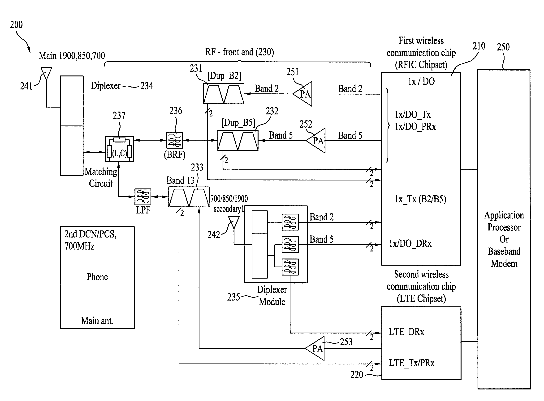
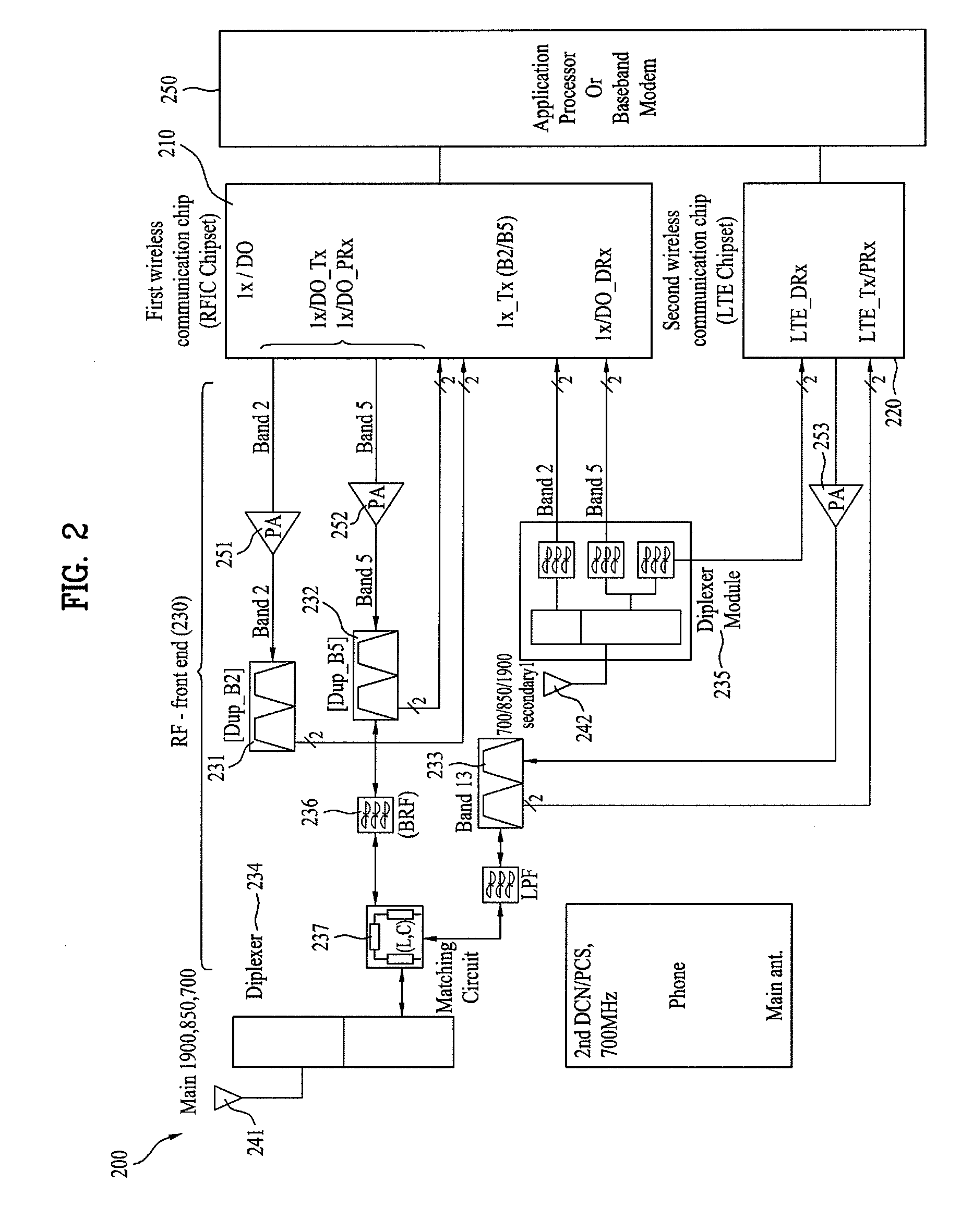
[0063]In particular, FIG. 2 is a diagram illustrating an example of a configuration of a user equipment 200 according to the second embodiment of the present invention. As shown in FIG. 2, the user equipment 200 includes a first wireless communication chip 210, a second wireless communication chip 220, an RF front-end module 230, a primary antenna 241, a secondary antenna 242, and an application processor or baseband modem 250.
[0064]The RF front-end module 230 also includes duplexers 231, 232 and 233, diplexers 234 and 235, band rejection filter (BRF) 236, a matching circuit module 237, and power amplifiers 251, 252 and 253.
[0065]The RF front-end module 230 according to this embodiment transmits signals of a plurality of frequency bands (for example, band 2 and band 5), which are output from the first wireless communication chip 210 and a signal (corresponding to band 13) output from the second wireless communication chip 220 to the primary antenna 241.
[0066]In more detail, the signals of the plurality of frequency bands (for example, band 2 and band 5), which are output from the first wireless communication chip 210 are respectively amplified by the power amplifiers 251 and 252, and the signal corresponding to the amplified band 2 and the signal corresponding to the amplified band 5 are transmitted to the primary antenna 241 through the matching circuit module 237 after the signal corresponding to the amplified band 2 passes through the duplexer 231 and the signal corresponding to the amplified band 5 passes through the duplexer 232. The signal corresponding to a specific frequency band (for example, band 13), which is output from the second wireless communication chip 220, is amplified through the power amplifier 239, processed through the duplexer 233 and the matching circuit module 237 and then transmitted to the primary antenna 241.
[0067]Since transmission characteristics due to impedance are greatly varied in the RF front-end module 230 if frequency becomes higher, it is preferable that impedance occurs uniformly at connection ends. However, because a characteristic impedance of 50Ω may not occur at respective ends in an actual design, impedance matching is used. The matching circuit module 237 serves to perform impedance matching. At this time, the Smith chart is used for normal impedance matching.
[0068]Further, the band rejection filter (BRF) 236 is located at a front end of the duplexers 231 and 232 in the RF Rx path and has a high IP3. The band rejection filter (BRF) 236 can reduce an influence of IM3 on the receiver by rejecting a transmitting signal, which directly affects IM3 occurring in the RF Rx path, to reach a specific level or less.
[0069]The RF front-end module 230 forwards the signals corresponding to specific frequency bands (for example, band 2 and band 5), which are externally received in the primary antenna 241, to the first wireless communication chip 210 through the duplexers 231 and 232, respectively. Also, the RF front-end module 230 forwards the signals corresponding to a specific frequency band (for example, band 13), which are externally received in the primary antenna 241, to the second wireless communication chip 220 through the duplexer 233.
[0070]In addition, the RF front-end module 230 forwards the signals corresponding to specific frequency bands (for example, band 2 and band 5), which are externally received in the secondary antenna 242, to the first wireless communication chip 210 through the diplexer 235. Further, the RF front-end module 230 forwards the signals corresponding to a specific frequency band (for example, band 13), which are externally received in the secondary antenna 242, to the second wireless communication chip 220 through the diplexer 235.
[0071]According to the aforementioned embodiments of the present invention, since transmission is performed through only one antenna, SAR can be reduced even if simultaneous signal transmission is performed through the plurality of frequency bands. Also, the influence of IM3 occurring due to simultaneous signal transmission through the plurality of frequency bands can be minimized. Moreover, it is possible to improve RF throughput while reducing complexity of the RF front-end.
[0072]The aforementioned embodiments are achieved by combination of structural elements and features of the present invention in a predetermined type. Each of the structural elements or features should be considered selectively unless specified separately. Each of the structural elements or features may be carried out without being combined with other structural elements or features.
[0073]Also, some structural elements and/or features may be combined with one another to constitute the embodiments of the present invention. The order of operations described in the embodiments of the present invention may be changed. Some structural elements or features of one embodiment may be included in another embodiment, or may be replaced with corresponding structural elements or features of another embodiment. Moreover, it will be apparent that some claims referring to specific claims may be combined with another claims referring to the other claims other than the specific claims to constitute the embodiment or add new claims by means of amendment after the application is filed.
[0074]The embodiments according to the present invention can be implemented by various ways, for example, hardware, firmware, software, or their combination. If the embodiment according to the present invention is implemented by hardware, the embodiment of the present invention can be implemented by one or more application specific integrated circuits (ASICs), digital signal processors (DSPs), digital signal processing devices (DSPDs), programmable logic devices (PLDs), field programmable gate arrays (FPGAs), processors, controllers, microcontrollers, microprocessors, etc.
[0075]If the embodiment according to the present invention is implemented by firmware or software, the embodiment of the present invention can be implemented by a type of a module, a procedure, or a function, which performs functions or operations described as above. A software code may be stored in a memory unit and then may be driven by a processor. The memory unit may be located inside or outside the processor to transmit and receive data to and from the processor through various means which are well known.
[0076]It will be apparent to those skilled in the art that the present invention can be embodied in other specific forms without departing from the spirit and essential characteristics of the invention. Thus, the above embodiments are to be considered in all respects as illustrative and not restrictive. The scope of the invention should be determined by reasonable interpretation of the appended claims and all change which comes within the equivalent scope of the invention are included in the scope of the invention.

PUM

no PUM

Description & Claims & Application Information

We can also present the details of the Description, Claims and Application information to help users get a comprehensive understanding of the technical details of the patent, such as background art, summary of invention, brief description of drawings, description of embodiments, and other original content. On the other hand, users can also determine the specific scope of protection of the technology through the list of claims; as well as understand the changes in the life cycle of the technology with the presentation of the patent timeline. Login to view more.

Similar technology patents

Task scheduling method and device based on multi-core system

InactiveCN102831011AImprove throughputImprove Thin ThroughputProgram initiation/switchingResource allocationCountermeasureOptimization system
Owner:SHANGHAI JIAO TONG UNIV

Classification and recommendation of technical efficacy words

  • Improve throughput
  • Remove influence

Device and method for processing photoacoustic signal

ActiveUS20140257079A1Remove influenceUltrasonic/sonic/infrasonic diagnosticsProcessing detected response signalPhysicsPhotoacoustic imaging in biomedicine
Owner:FUJIFILM CORP
Why Eureka
Try Eureka