ENHANCED PLANARITY IN GaN EDGE EMITTING LASERS

a laser and edge technology, applied in lasers, semiconductor devices, semiconductor lasers, etc., can solve the problems of non-planar quantum wells, excessive optical loss, and non-uniform thickness and/or content, and achieve the effects of reducing gain, broadening emission spectrum, and increasing radiative efficiency

Inactive Publication Date: 2011-12-01
THORLABS QUANTUM ELECTRONICS
View PDF3 Cites 2 Cited by
  • Summary
  • Abstract
  • Description
  • Claims
  • Application Information

AI Technical Summary

Benefits of technology

[0002]The present inventors have recognized that long wavelength light emitting devices grown on semi-polar GaN substrates can exhibit increased radiative efficiency. For example, efficient green laser diodes can be grown on semi-polar 20 21 GaN substrates and can result in homogeneous GaInN quantum wells even at high In composition. The present inventors have also recognized that in many cases it is difficult to maintain planarity in hetero-epitaxial GaInN and AlGaInN layers grown on GaN substrates in such devices. More specifically, for many long wavelength light emitting devices grown on semi-polar GaN substrates, some of the layers, particularly those grown at low temperature and containing In, show faceting and undulation. These undulations can lead to non planar quantum wells with non uniform thickness and / or non-uniform In content. The resulting laser structure can become highly non-planar and the non-planarity of the waveguiding and cladding layers in particular can lead to excessive optical loss. In quantum wells, thickness non-uniformity and variations in the Indium content can reduce gain and broaden the emission spectrum.

Problems solved by technology

These undulations can lead to non planar quantum wells with non uniform thickness and / or non-uniform In content.
The resulting laser structure can become highly non-planar and the non-planarity of the waveguiding and cladding layers in particular can lead to excessive optical loss.

Method used


Image

  • ENHANCED PLANARITY IN GaN EDGE EMITTING LASERS
  • ENHANCED PLANARITY IN GaN EDGE EMITTING LASERS

Examples


Embodiment Construction

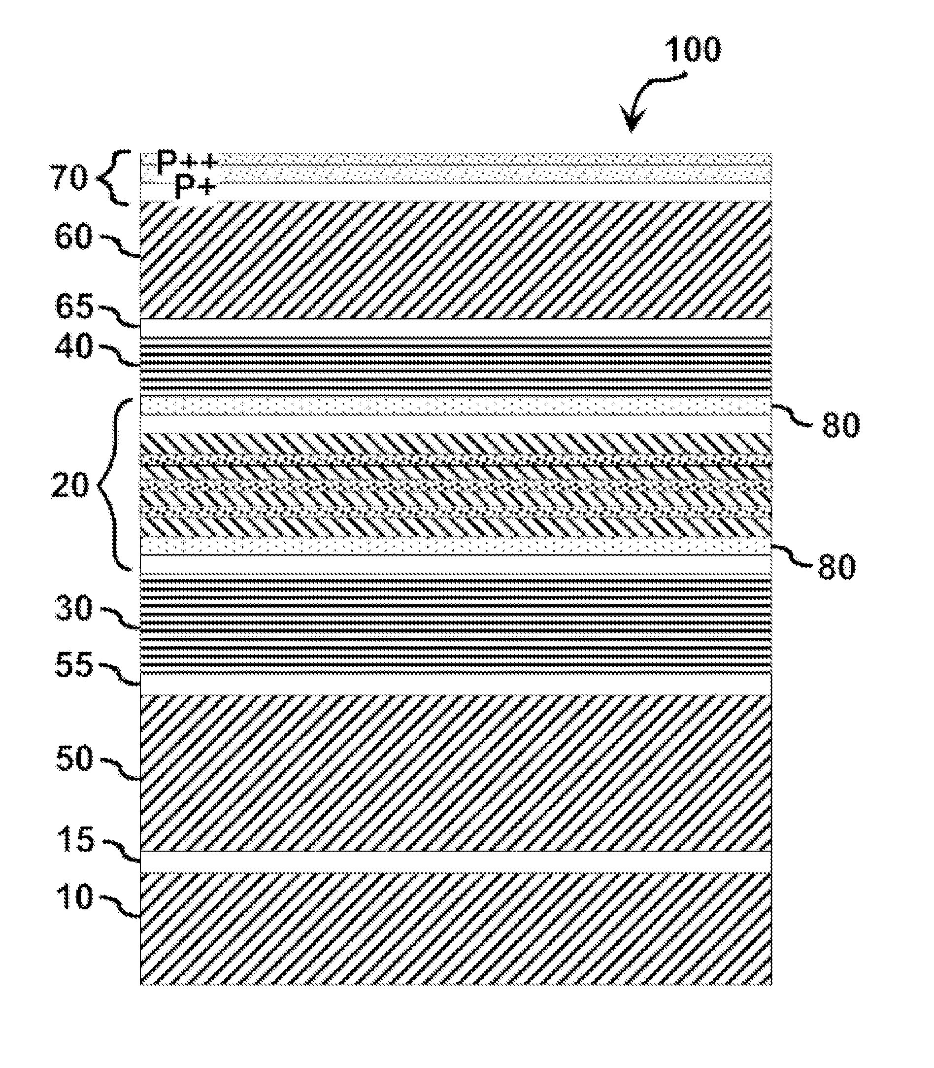
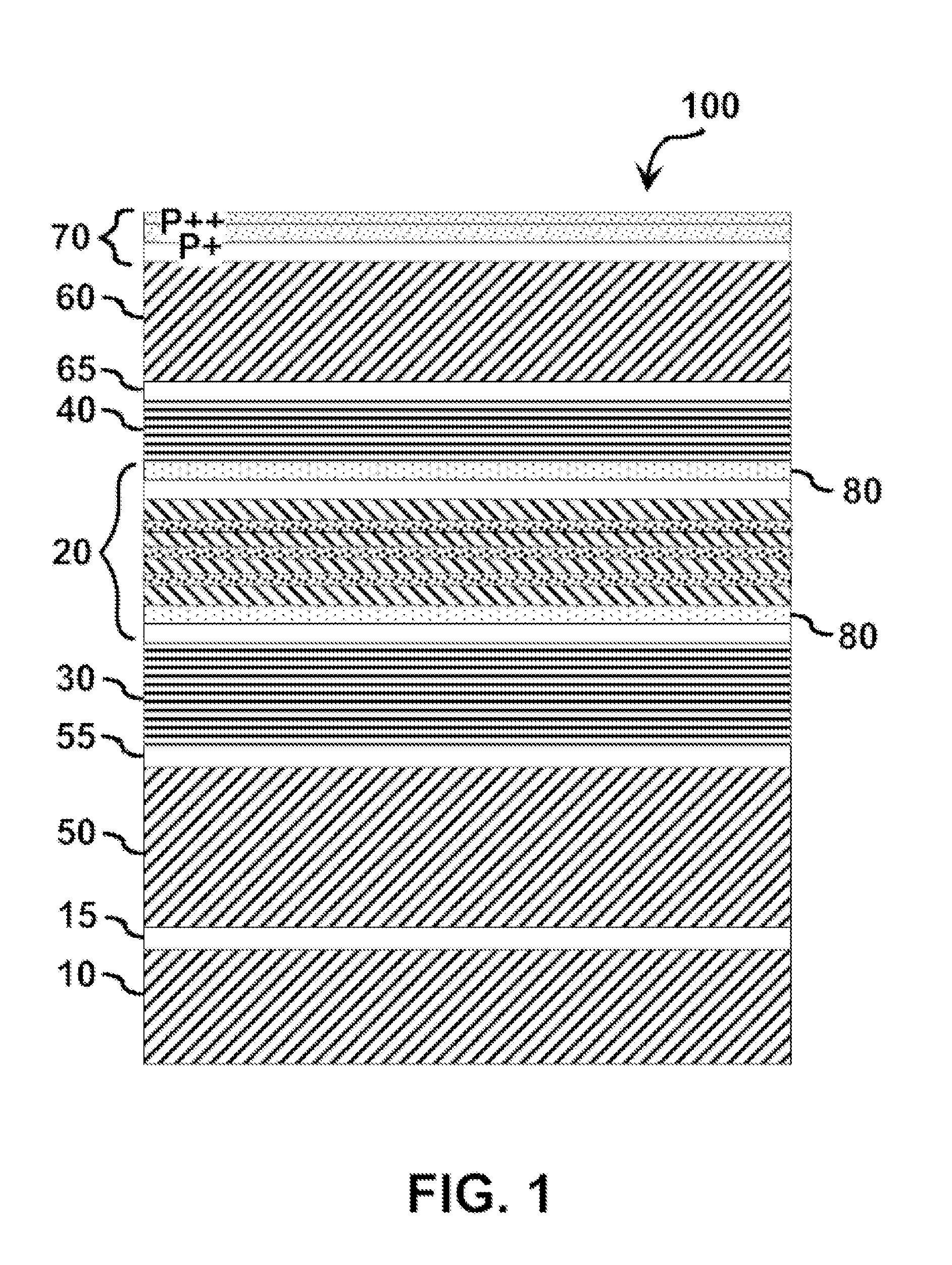
[0006]Referring initially to FIG. 1, a GaN edge emitting laser 100 is illustrated comprising a semi-polar GaN substrate 10, an active region 20, an N-side waveguiding layer 30, a P-side waveguiding layer 40, an N-type cladding layer 50, and a P-type cladding layer 60. The GaN substrate defines a 20 21 crystal growth plane and a glide plane. For the purposes of describing and defining the present invention, it is noted that GaN lasers are often grown on the polar plane of a GaN substrate, which imposes strong internal fields that can hamper electron-hole recombination needed for light emission. The non-polar planes, such as the m-plane and a-plane, can be used to eliminate these fields. GaN substrates can also be cut along semi-polar crystal planes, creating much weaker internal fields and allowing for a high indium concentration in the active region, which can stretch emission wavelengths to green. Particular embodiments of the present disclosure relate to growth on the 20 21 crysta...


PUM


Abstract

A GaN edge emitting laser is provided comprising a semi-polar GaN substrate, an active region, an N-side waveguiding layer, a P-side waveguiding layer, an N-type cladding layer, and a P-type cladding layer. The GaN substrate defines a 20 21 crystal growth plane and a glide plane. The N-side and P-side waveguiding layers comprise a GaInN/GaN or GaInN/GaInN superlattice (SL) waveguiding layers. The superlattice layers of the N-side and P-side SL waveguiding layers define respective layer thicknesses that are optimized for waveguide planarity, the layer thicknesses being between approximately 1 nm and approximately 5 nm. In accordance with another embodiment of the present disclosure, planarization can be enhanced by ensuring that the N-side and P-side GaN-based waveguiding layers are grown at a growth rate that exceeds approximately 0.09 nm/s, regardless of whether the N-side and P-side GaN-based waveguiding layers are provided as a GaInN/GaN or GaInN/GaInN SL or as bulk waveguiding layers. In still further embodiments, planarization can be enhanced by selecting optimal SL layer thicknesses and growth rates. Additional embodiments are disclosed and claimed.

Description

BACKGROUND[0001]The present disclosure relates to GaN edge emitting lasers and, more particularly, to schemes for enhancing planarity in such lasers.BRIEF SUMMARY[0002]The present inventors have recognized that long wavelength light emitting devices grown on semi-polar GaN substrates can exhibit increased radiative efficiency. For example, efficient green laser diodes can be grown on semi-polar 20 21 GaN substrates and can result in homogeneous GaInN quantum wells even at high In composition. The present inventors have also recognized that in many cases it is difficult to maintain planarity in hetero-epitaxial GaInN and AlGaInN layers grown on GaN substrates in such devices. More specifically, for many long wavelength light emitting devices grown on semi-polar GaN substrates, some of the layers, particularly those grown at low temperature and containing In, show faceting and undulation. These undulations can lead to non planar quantum wells with non uniform thickness and / or non-unif...

Claims


Application Information

Patent Timeline
Patent Type & Authority Applications(United States)
IPC IPC(8): H01S5/343H01S5/34H01L33/04
CPCB82Y20/00H01S5/3201H01S5/34333H01S5/3216H01S5/3202H01S5/320275H01S5/10H01S5/343
Inventor BHAT, RAJARAM
Owner THORLABS QUANTUM ELECTRONICS
Why Eureka
Try Eureka