

Plasma processing apparatus and sample stage
a technology of processing apparatus and sample stage, which is applied in the direction of superimposed coating process, metal material coating process, coating, etc., can solve the problems of increasing the heat capacity of the ceramic member, the distance between the heater and the wafer becomes larger, and it is difficult to directly measure the temperature of the wafer with high accuracy, so as to improve the uniformity of the temperature of the wafer, improve the uniformity of the wafer, and improve the accuracy of the distribution
- Summary
- Abstract
- Description
- Claims
- Application Information
AI Technical Summary
Benefits of technology
Problems solved by technology
Method used
Image

Examples
Embodiment Construction
[0019]Referring now to the drawings, description will be given of an embodiment according to the present invention.
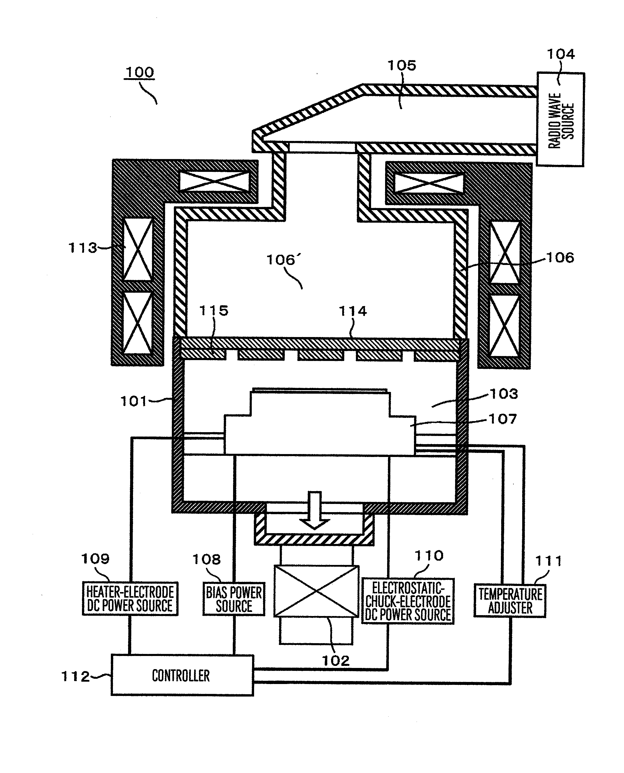
[0020]FIG. 1 is a view of a longitudinal section to explain an outline of a configuration of a plasma processing apparatus according to the present invention. The plasma processing apparatus 100 shown in FIG. 1 includes a vacuum vessel 101, an electromagnetic field supply unit disposed at a position over the vacuum vessel 101, the position being in an outer periphery thereof, to supply an electric field or a magnetic field to the vacuum vessel 101, and an exhaust unit disposed below the vacuum vessel 101 to exhaust gases therefrom.
[0021]In the vacuum vessel 101, there are arranged a processing chamber 103 in which plasma is generated and a sample as a processing object is processed by the plasma and a sample stage 107 having a surface on which the sample is placed and is held. Over the vacuum vessel 101, there are arranged a radio wave source 104, for example, a magnetr...
PUM
| Property | Measurement | Unit |
|---|---|---|
| Length | aaaaa | aaaaa |
| Length | aaaaa | aaaaa |
Abstract
Description
Claims
Application Information