Power semiconductor system

Inactive Publication Date: 2011-12-08
KK TOSHIBA
View PDF0 Cites 30 Cited by
  • Summary
  • Abstract
  • Description
  • Claims
  • Application Information

AI Technical Summary

Problems solved by technology

Further, both of the elements are sometimes disposed monolithically within the same chip an...

Method used


Image

  • Power semiconductor system
  • Power semiconductor system
  • Power semiconductor system

Examples


working example 1

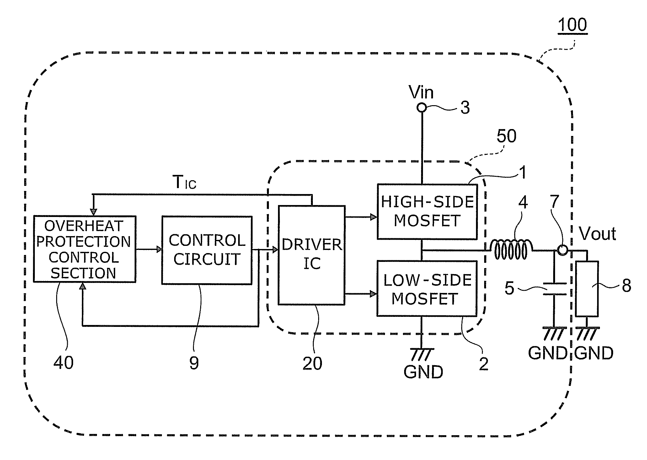
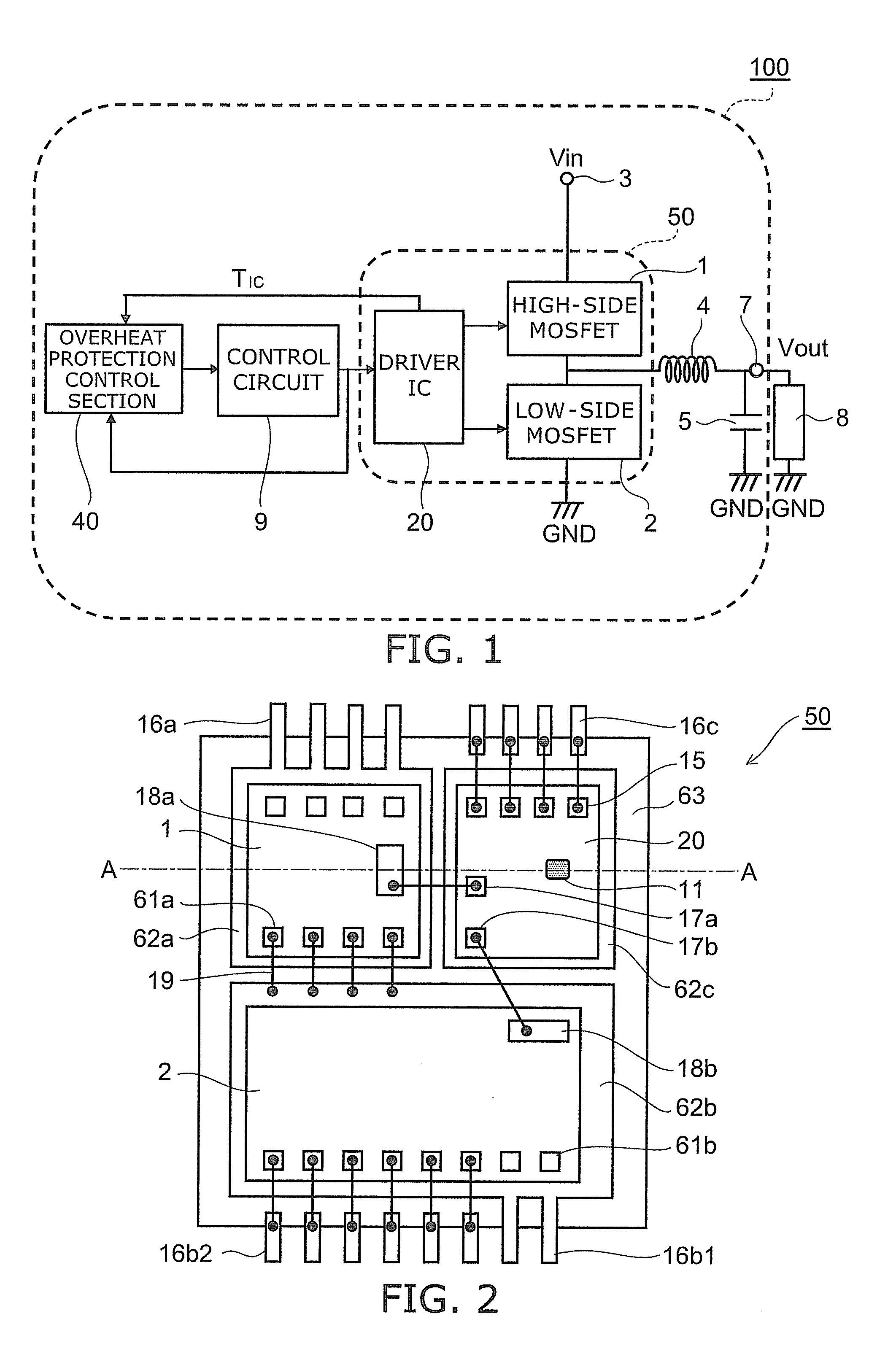
FIG. 1 is a block diagram showing the main configuration of a DC-DC convertor 100 which is an example of a power semiconductor system of a working example 1.

FIG. 2 is a plan view showing an example of a packaged part of the main configuration in the DC-DC convertor 100 which is an example of the power semiconductor system of the working example 1.

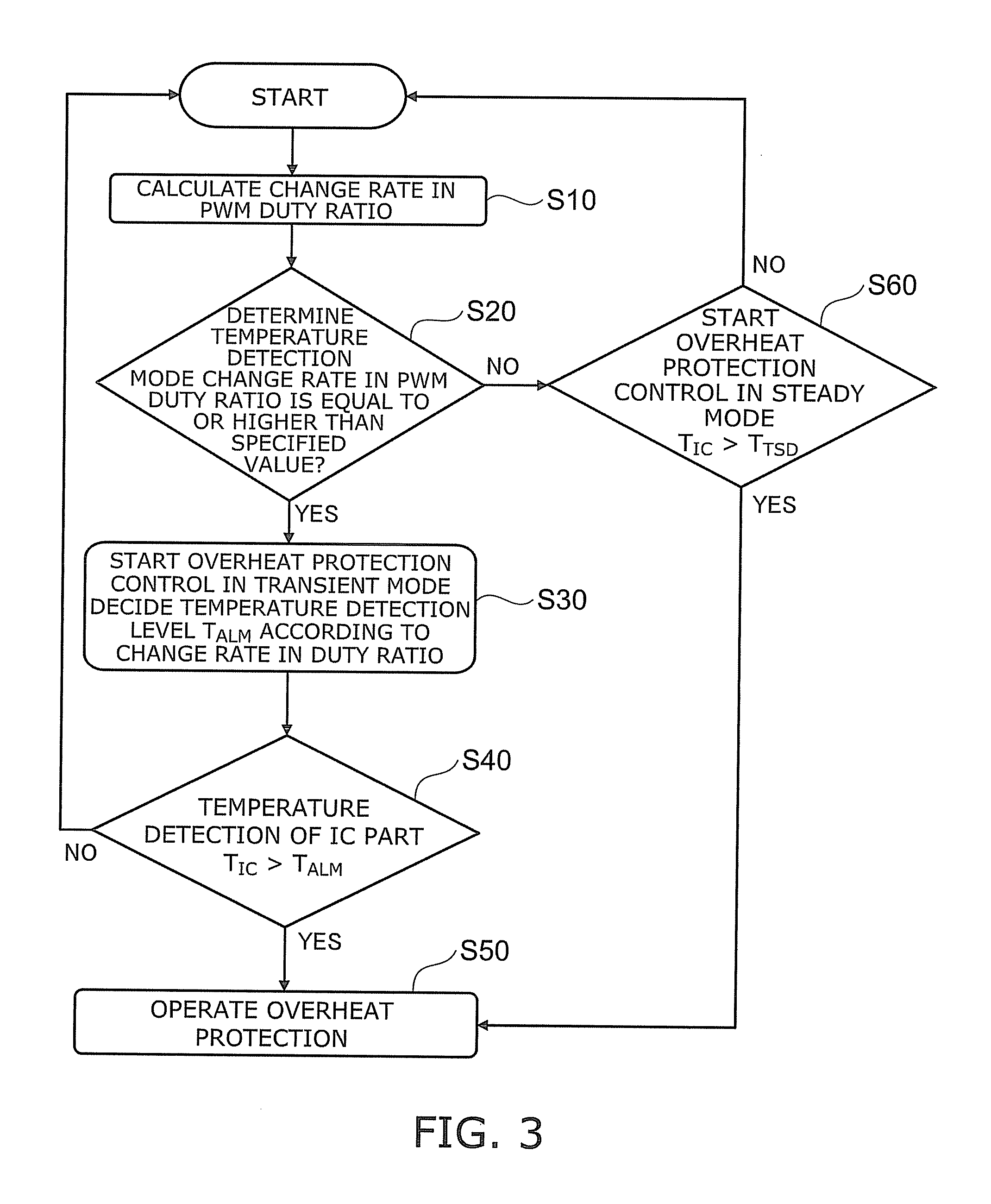
FIG. 3 is a flowchart showing overheat protection control of the DC-DC convertor 100 the working example 1.

As shown in FIG. 1, the DC-DC convertor 100 of the working example 1 includes a first power semiconductor element 1, a second power semiconductor element 2, an input terminal 3 of the DC-DC convertor, an inductor 4, a capacitor 5, a ground terminal GND, an output terminal 7 of the DC-DC convertor, a driver IC 20, a control circuit 9, and an overheat protection control section 40. Note that, while an example of the power semiconductor element will be explained for a case in which an n-channel MOSFET is used, it is possible to use an IGB...

working example 2

A working example 2 will be described by the use of FIG. 7 to FIG. 11. FIG. 7 is a block diagram showing a main configuration of a DC-DC convertor which is an example of a power semiconductor system of the working example 2. FIG. 8 is a plan view of a power semiconductor device 51 which packages a part of the main configuration of the DC-DC convertor which is an example of the power semiconductor system of the working example 2. FIG. 9 is a flowchart showing the overheat protection control of the DC-DC convertor 200 of the working example 2. Note that the same reference numeral is used for a part having the same configuration as that described in the working example 1 and explanation thereof will be omitted.

As shown in FIG. 7, the DC-DC convertor 200 of the working example 2 includes a first power semiconductor element 1, a second power semiconductor element 2, an input terminal 3 of the DC-DC convertor, an inductor 4, a capacitor 5, an output terminal 7 of the DC-DC convertor, a gr...

working example 3

A DC-DC convertor 300 of a working example 3 will be explained. Note that a part having the same configuration as the configuration explained in the working example 1 is denoted by the same reference numeral and explanation thereof will be omitted. The DC-DC convertor 300 which is an example of a power semiconductor system of the working example 3 is different from that of the working example 1 in a power semiconductor device 53 which is an MCM including the elements within the same resin package. The configuration of the DC-DC convertor is the same as that of the working example 1 shown in FIG. 1, and the flow of the overheat protection control is also the same as that of the working example 1 shown in FIG. 3. FIG. 14 shows a plan view of the power semiconductor device 53 of the working example.

The DC-DC convertor 300 of the working example is different from the DC-DC convertor 100 of the working example 1 in the following point. The working example is different from the working ex...


PUM


Abstract

According to one embodiment, a power semiconductor system includes; a first power semiconductor element, a driver IC, a first temperature detection element, a control circuit and an overheat protection control section. The first power semiconductor element controls current flowing between a first electrode and a second electrode with a control electrode. The driver IC supplies a drive signal making the first power semiconductor element on and off. The first temperature detection element detects a temperature of the driver IC. The control circuit supplies a control signal for controlling operation of the driver IC to the driver IC. The overheat protection control section is configured to supply an overheat protection signal to the control circuit based on an output of the first temperature detection element. The control circuit performs overheat protection operation. The overheat protection control section supplies the overheat protection signal to the control circuit.

Description

CROSS-REFERENCE TO RELATED APPLICATIONSThis application is based upon and claims the benefit of priority from the prior Japanese Patent Application No. 2010-129663, filed on Jun. 7, 2010; the entire contents of which are incorporated herein by reference.FIELDEmbodiments described herein relate generally to a power semiconductor system.BACKGROUNDIn a DC-DC converter used for a power supply of a personal computer, a home electric appliance, etc., an inverter used for motor control, and the like, a power semiconductor system is configured including a control circuit, a driver IC, a power semiconductor element, and the like, for performing switching control. For the power semiconductor element, there is used a high voltage MOSFET (Metal Oxide Semiconductor Field Effect Transistor), for example. Then, a power semiconductor device called a MCM (Multi Chip Module) is sometimes formed which includes a high-side MOSFET, a low-side MOSFET, and a driver IC for turning on and off the gate elect...

Claims


Application Information

Patent Timeline
IPC IPC(8): H03K3/011
CPCH03K17/6871H03K19/00369H03K2017/0806H01L2224/48137H01L2224/48247H01L2924/1305H01L2924/13055H01L2924/13091H01L2924/00H01L2224/05554H01L2224/0603
Inventor ENDO, KOICHITSUNETSUGU, YUKIONAKAMURA, KAZUTOSHI
Owner KK TOSHIBA
Why Eureka
Try Eureka