System architecture design for time-of- flight system having reduced differential pixel size, and time-of- flight systems so designed

a time-of-flight system and differential pixel technology, applied in distance measurement, instruments, surveying and navigation, etc., can solve the problems of increasing the complexity of asynchronous reset, reducing the array region of ic chip area required to fabricate or implement pixels, and substantially no capacitor or component mismatch effect of the accuracy of res

Active Publication Date: 2011-12-15
MICROSOFT TECH LICENSING LLC
View PDF3 Cites 25 Cited by
  • Summary
  • Abstract
  • Description
  • Claims
  • Application Information

AI Technical Summary

Benefits of technology

[0050]Embodiments of the present invention provide methods to produce a high performance, feature rich TOF system, phase-based or otherwise using small TOF pixels that may detect single-ended or preferably differentially. The array region of IC chip area required to fabricate or implement the pixels is reduced by intelligently off-loading or removing from within the pix...

Problems solved by technology

Further, capacitor or component mismatch has substantially no effect on the accuracy of the reset.
This is what occurs in the second read-out method, but unfortunately a charge error is created whenever the initial amplifier input was not precisely Vref3.
Generally, an asynchronous reset is more complex as each pixel must constantly monitor its differential signal capacitor voltage, and self generate control signals required to adjust the CDSC voltage.
Further, if the reset count is not accumulated inside the pixel, the occurrence of resets may need to be communicated asynchronously, a difficult task when all pixels simultaneously reset.
Thus, all things ...

Method used


Image

  • System architecture design for time-of- flight system having reduced differential pixel size, and time-of- flight systems so designed
  • System architecture design for time-of- flight system having reduced differential pixel size, and time-of- flight systems so designed
  • System architecture design for time-of- flight system having reduced differential pixel size, and time-of- flight systems so designed

Examples


Embodiment Construction

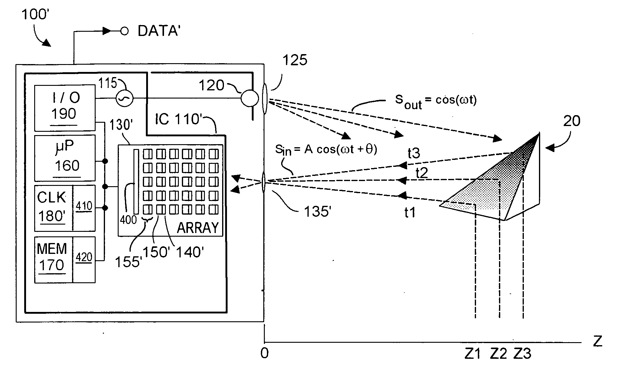
[0082]FIG. 8 depicts a generic TOF system 100′, designed according to embodiments of the present invention. Preferably the area size required to implement individual pixels 155′ within array 130′ on IC chip 110′ is reduced relative to prior art pixels described earlier herein. Note too the reduced size of optical system 135′ as compared with optical system 135 in FIG. 1A. The smaller pixel size in array 130′ in FIG. 8 can result in thinner and smaller diameter optics 135′.

[0083]System 100′ in FIG. 8 benefits from reduced pixel area size by advantageously intelligently off-loading or removing from within the pixel certain circuitry, components, and / or functionality that in the prior art would be present in each dedicated detector electronics. In FIG. 8, 150′ denotes the reduced-area electronics associated with each detector 140′ in the array. In FIG. 8, block 400 denotes the off-loaded circuitry, components, and / or functionality that would otherwise be present in the dedicated el...


PUM


Abstract

Embodiments of the present invention provide methods to produce a high performance, feature rich TOF system, phase-based or otherwise using small TOF pixels, single-ended or preferably differential, as well as TOF systems so designed. IC chip area required for pixels is reduced by intelligently off-loading or removing from within the pixel certain components and/or functionality. In some embodiments during a single TOF system capture period, analog values from each pixel are repeatedly sampled and converted to digital values, which are combined and manipulated on the sensor chip. Combining this plurality of values enables appropriately compact data from the sensor chip. Embodiments of the present invention implement a TOF system with high ambient light resilience, high dynamic range, low motion blur and dealiasing support, while advantageously reducing pixel area size relative to prior art TOF pixels.

Description

RELATIONS TO CO-PENDING APPLICATION[0001]This is a continuation application from co-pending U.S. provisional patent application Ser. No. 61,133,647 filed on 30 Jun. 2008, entitled System Architecture Design for Time-of-Flight System Having Reduced Differential Pixel Size, and Time-of-Flight Systems So Designed, which application is assigned to Canesta, Inc. of Sunnyvale, Calif., assignee herein.FIELD OF THE INVENTION[0002]The present invention relates generally to time-of-flight (TOF) systems, and more particularly to designing improved architecture for such TOF systems to reduce size of the preferably differential pixels used in such systems, and TOF systems so designed.BACKGROUND OF THE INVENTION[0003]Modern time-of-flight (TOF) systems can ascertain depth distances Z to a target object by emitting modulated optical energy of a known phase, and examining phase-shift in the optical signal reflected from the target object, the phase-shift being detected by an array that includes pix...

Claims


Application Information

Patent Timeline
IPC IPC(8): G01C3/08G01S7/491G01S7/4914G01S17/894
CPCG01S7/4914G01S17/36G01S7/491G01C3/08G01S17/89G01S17/894
Inventor BAMJI, CYRUSMEHTA, SWATI
Owner MICROSOFT TECH LICENSING LLC
Why Eureka
Try Eureka