

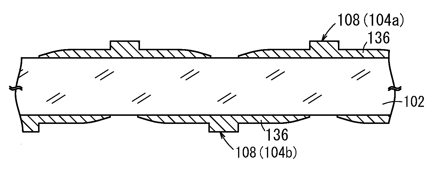
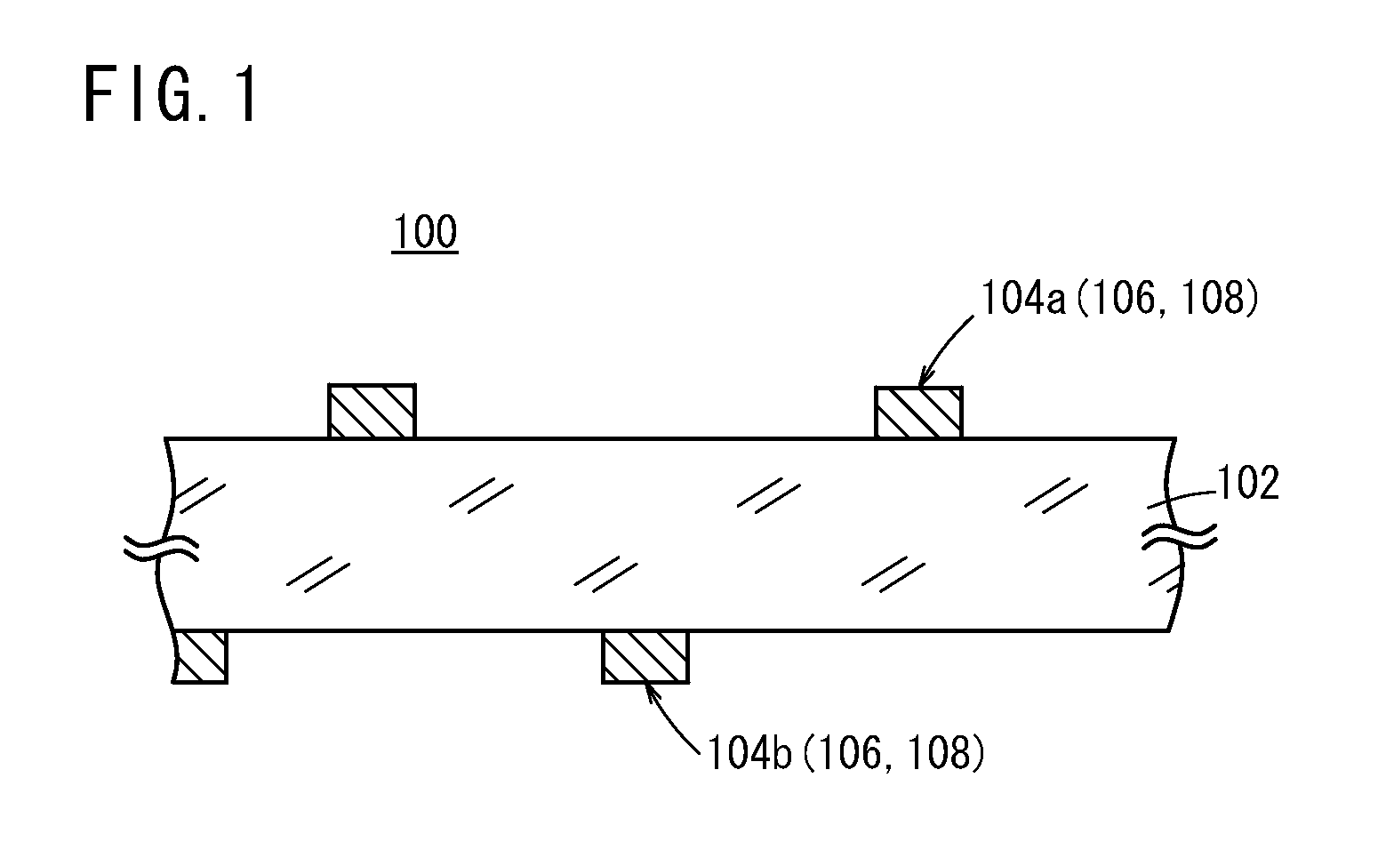
Conductive film and method for producing the same
a technology of conductive film and film, applied in the field of conductive film, can solve the problems of dye deterioration of the conductive properties of the developed layer, inability to obtain the desired conductivity, and disadvantageous blue image on the back side of the transparent support, so as to prevent the generation of moire and improve the conductivity of the conductive pattern
- Summary
- Abstract
- Description
- Claims
- Application Information
AI Technical Summary
Benefits of technology
Problems solved by technology
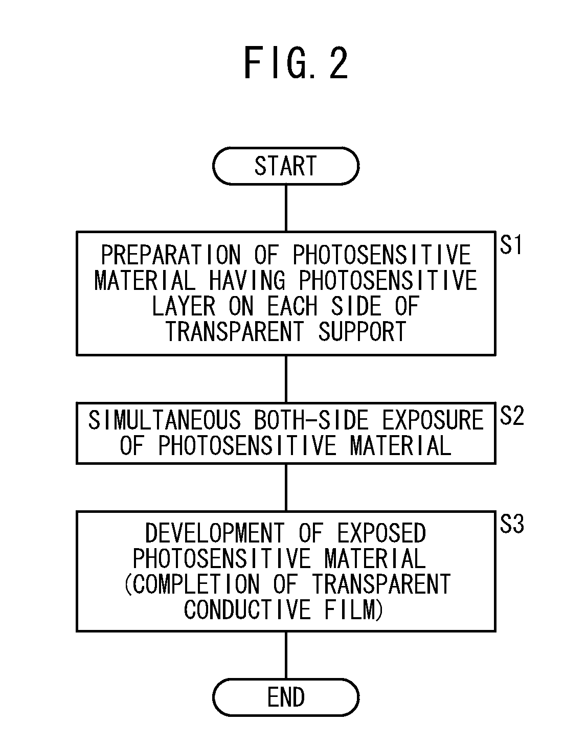
Method used
Image

Examples
example 1
(Photosensitive Silver Halide Material)
[0170]An emulsion containing an aqueous medium, a gelatin, and silver iodobromochloride particles was prepared. The amount of the gelatin was 20.0 g per 150 g of Ag, and the silver iodobromochloride particles had an I content of 0.2 mol %, a Br content of 40 mol %, and an average spherical equivalent diameter of 0.1 μm.
[0171]K3Rh2Br9 and K2IrCl6 were added to the emulsion at a concentration of 10−7 mol / mol-silver to dope the silver bromide particles with Rh and Ir ions. The emulsion and a gelatin hardener were applied to the transparent support 102 composed of a polyethylene terephthalate (PET). The applied silver amount was 8 g / m2, the coverage of the silver halide particles with the spectral sensitizing dye was 20% or less, and the silver / binder (gelatin) volume ratio was 1 / 1. The applied emulsion had a surface resistance value (log SR) of 15 and a high contrast photographic property with a gamma of 4 or more.
[0172]The transparent support 102...
examples 2 and 3
[0177]Conductive films of Examples 2 and 3 were produced in the same manner as Example 1 except that the silver / binder volume ratios of the emulsions were 2 / 1 and 3 / 1 respectively.
examples 4 to 6
[0178]Conductive films of Examples 4 to 6 were produced in the same manner as Example 1 except that the silver / binder volume ratios of the emulsions were 3 / 1 (Example 5) and 4 / 1 (Examples 4 and 6) and that the surface resistance values (log SR) of the emulsion layers on the photosensitive silver halide materials were set at 10 (Example 6), 11 (Example 4), and 13 (Example 5) by controlling the salt concentration of the emulsions.
PUM
| Property | Measurement | Unit |
|---|---|---|
| width | aaaaa | aaaaa |
| length | aaaaa | aaaaa |
| resistance | aaaaa | aaaaa |
Abstract
Description
Claims
Application Information