Light emitting diode

a light-emitting diode and light-emitting technology, applied in the direction of basic electric elements, electrical equipment, semiconductor devices, etc., can solve the problems of light proceeding for a considerable distance, light loss, and light scattering, and achieve the effect of improving light extraction efficiency

Active Publication Date: 2011-12-29
SEOUL VIOSYS CO LTD
View PDF8 Cites 26 Cited by
  • Summary
  • Abstract
  • Description
  • Claims
  • Application Information

AI Technical Summary

Benefits of technology

[0013]Exemplary embodiments of the present invention provide an LED having improved light extraction efficiency.
[0014]Exemplary embodiments of the present invention also provide an LED having improved luminous efficiency by improving light reflectance.

Problems solved by technology

However, until the light generated in the active layer is scattered on a surface of the sapphire substrate, the light may proceed for a considerable distance within the nitride semiconductor layers.
Accordingly, since a light path may be lengthened, light loss may occur, and a portion of the scattered light is may be trapped in the nitride semiconductor layers by internal total reflection.
This reflectance is relatively high, but light loss may still occur even when the reflection metal layer is formed.

Method used


Image

  • Light emitting diode
  • Light emitting diode
  • Light emitting diode

Examples


Embodiment Construction

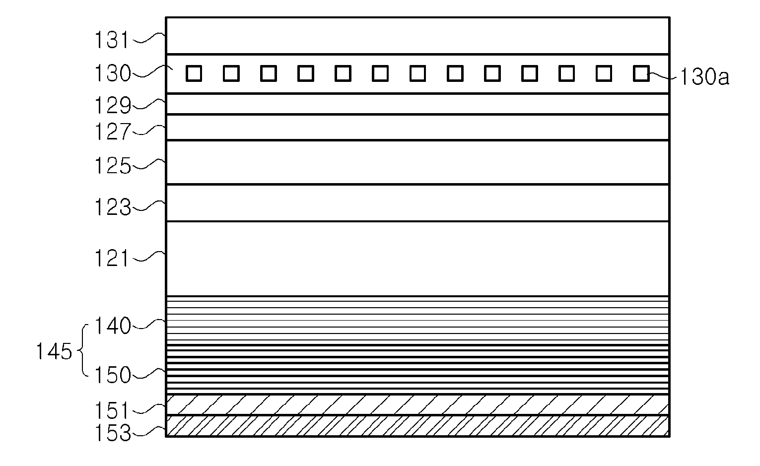
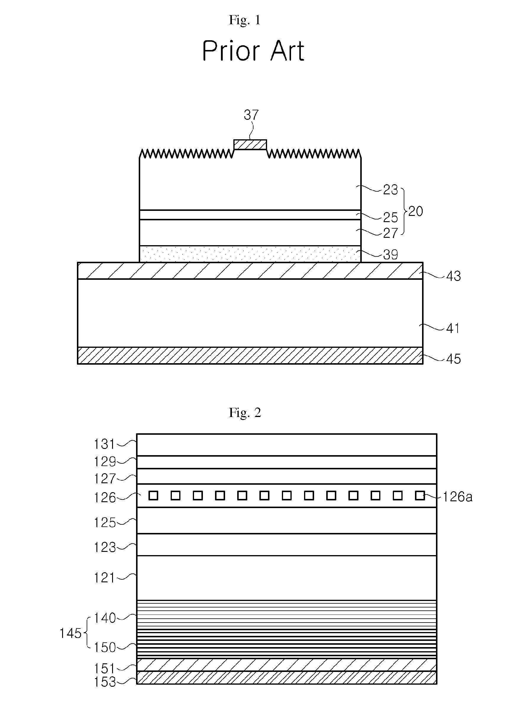
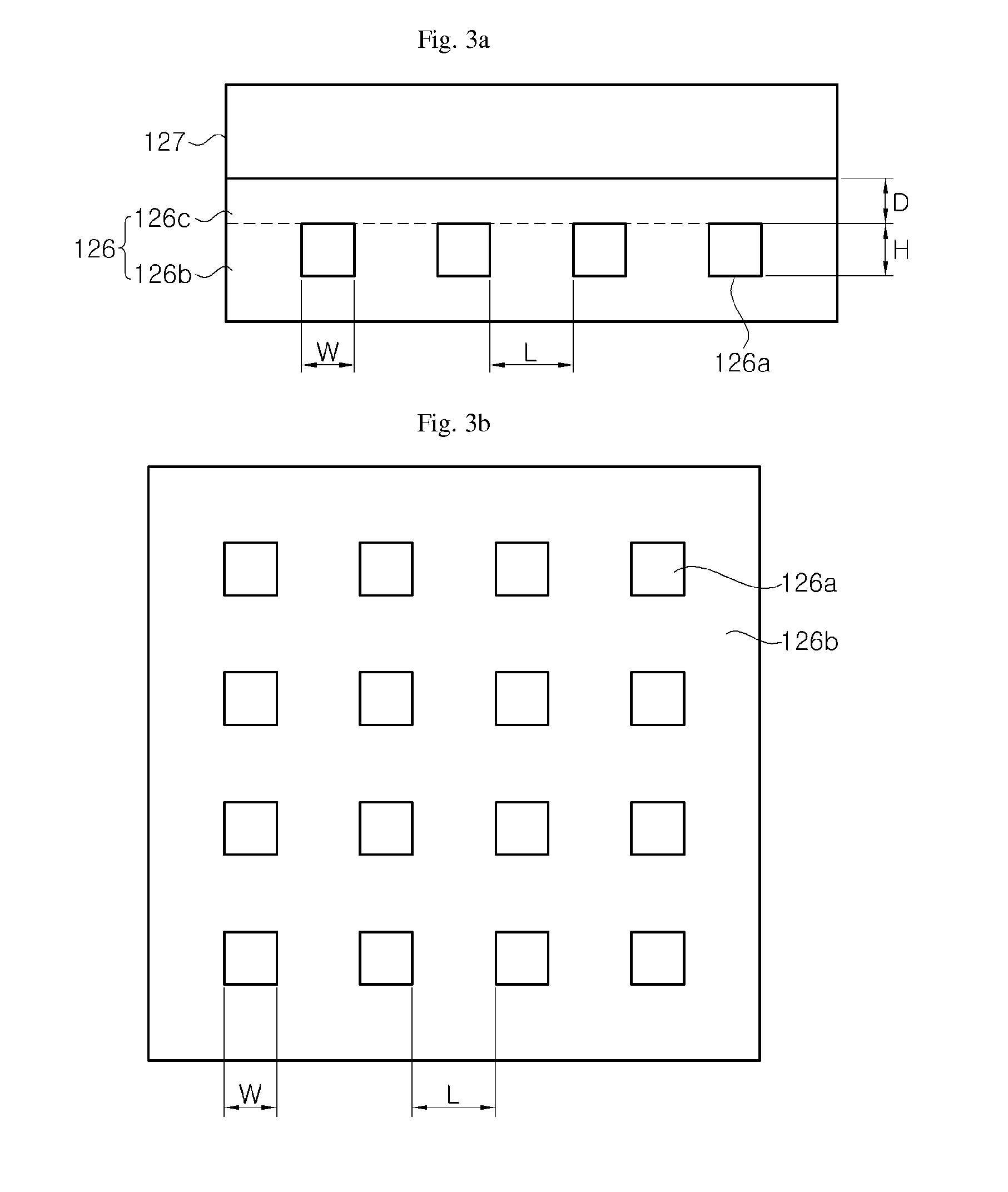
[0033]Hereinafter, preferred embodiments of the present invention will be described in detail with reference to the accompanying drawings. The following embodiments are provided only for illustrative purposes so that those skilled in the art can fully understand the spirit of the present invention. Therefore, the present invention is not limited to the following embodiments but may be implemented in other forms. In the drawings, the widths, lengths, thicknesses and the like of elements may be exaggerated for convenience of illustration. Like reference numerals indicate like elements throughout the specification and drawings.

[0034]It will be understood that when an element or layer is referred to as being “on” or “connected to” another element or layer, it can be directly on or directly connected to the other element or layer, or intervening elements or layers may be present. In contrast, when an element is referred to as being “directly on” or “directly connected to” another element...


PUM


Abstract

An exemplary embodiment of the present invention relates to a light emitting diode (LED) including a substrate, a first nitride semiconductor layer arranged on the substrate, an active layer arranged on the first nitride semiconductor layer, a second nitride semiconductor layer arranged on the active layer, a third nitride semiconductor layer disposed between the first nitride semiconductor layer or between the second nitride semiconductor layer and the active layer, the third nitride semiconductor layer comprising a plurality of scatter elements within the third nitride semiconductor layer, and a distributed Bragg reflector (DBR) comprising a multi-layered structure, the substrate being arranged between the DBR and the third nitride semiconductor layer.

Description

CROSS-REFERENCE TO RELATED APPLICATIONS[0001]This application claims priority from and the benefit of Korean Patent Application No. 10-2010-0059861, filed on Jun. 24, 2010 and Korean Patent Application No. 10-2010-0072821, filed on Jul. 28, 2010, which are hereby incorporated by reference for all purposes as if fully set forth herein.BACKGROUND OF THE INVENTION[0002]1. Field of the Invention[0003]Exemplary embodiments of the present invention relate to a light emitting diode (LED), and more particularly, to an LED having improved light extraction efficiency.[0004]2. Description of the Related Art[0005]Gallium nitride (GaN)-based LEDs are widely used for display elements and backlights. Further, LEDs may have lower electric power consumption and a longer lifetime as compared with conventional light bulbs or fluorescent lamps, so that their applications have been expanded into general illumination while substituting for conventional incandescent bulbs and fluorescent lamps. Particular...

Claims


Application Information

Patent Timeline
Patent Type & Authority Applications(United States)
IPC IPC(8): H01L33/10
CPCH01L33/10H01L33/025H01L2933/0091
Inventor KIM, CHANG YOUNLEE, JOON HEEYOU, JONG KYUNLIM, HONG CHOLKIM, HWA MOK
Owner SEOUL VIOSYS CO LTD
Why Eureka
Try Eureka