Bipolar transistor having self-adjusted emitter contact

a transistor and self-adjusting technology, applied in the field of bipolar semiconductor memory devices, can solve the problems of inability to design the dimensions of overlap, inability to adjust the extent of lateral overhang of the horizontal bar of the t-shaped emitter self-adjustment, etc., to improve the high-frequency characteristics of the transistor, reduce distance and dimension, and low parasitic base-emitter capacitance

Active Publication Date: 2012-01-05
IHP GMBH INNOVATIONS FOR HIGH PERFORMANCE MICROELECTRONICS LEIBNIZ INST FUR INNOVATIVE
View PDF2 Cites 30 Cited by
  • Summary
  • Abstract
  • Description
  • Claims
  • Application Information

AI Technical Summary

Benefits of technology

[0051]The semiconductor device according to the invention is distinguished by its bipolar transistor having especially good high-frequency characteristics. These are achieved by a reduced resistance of the base connection region, which due to the inventive structure, especially when using the inventive method described below, is accompanied by an especially low parasitic base-emitter capacitance of the bipolar transistor.
[0091]In this embodiment, only part of the base connection region is initially grown by selective epitaxial growth, after which the vertical distance between the insulating layer and the second auxiliary layer is increased by isotropic etching, so that the remaining part of the base connection region is produced by selective or differential epitaxy. It is possible in this way to achieve a greater outward layer thickness for the base connection than in the inner region, as a result of which the resistance of the base connection region can be reduced.

Problems solved by technology

As a consequence, it has not been possible until now to self-align the width of lateral overlapping of the generally T-shaped emitter with the base connection region that laterally adjoins the base, in a manner than is independent of other important dimensions of the transistor.
More specifically, it has not been possible to adjust the extent of lateral overhang of the horizontal bar of the T-shaped emitter self-aligningly with the emitter window, without altering the gap between the emitter window and the base connection region at the same time.
This leads to a situation in which the dimensions of the overlap cannot be designed without taking account of the error tolerances associated with the photolithographic process.
The aforementioned disadvantages of the prior art stand in the way of any further improvements in the high-frequency characteristics of a bipolar transistor.

Method used


Image

  • Bipolar transistor having self-adjusted emitter contact
  • Bipolar transistor having self-adjusted emitter contact
  • Bipolar transistor having self-adjusted emitter contact

Examples


example 1

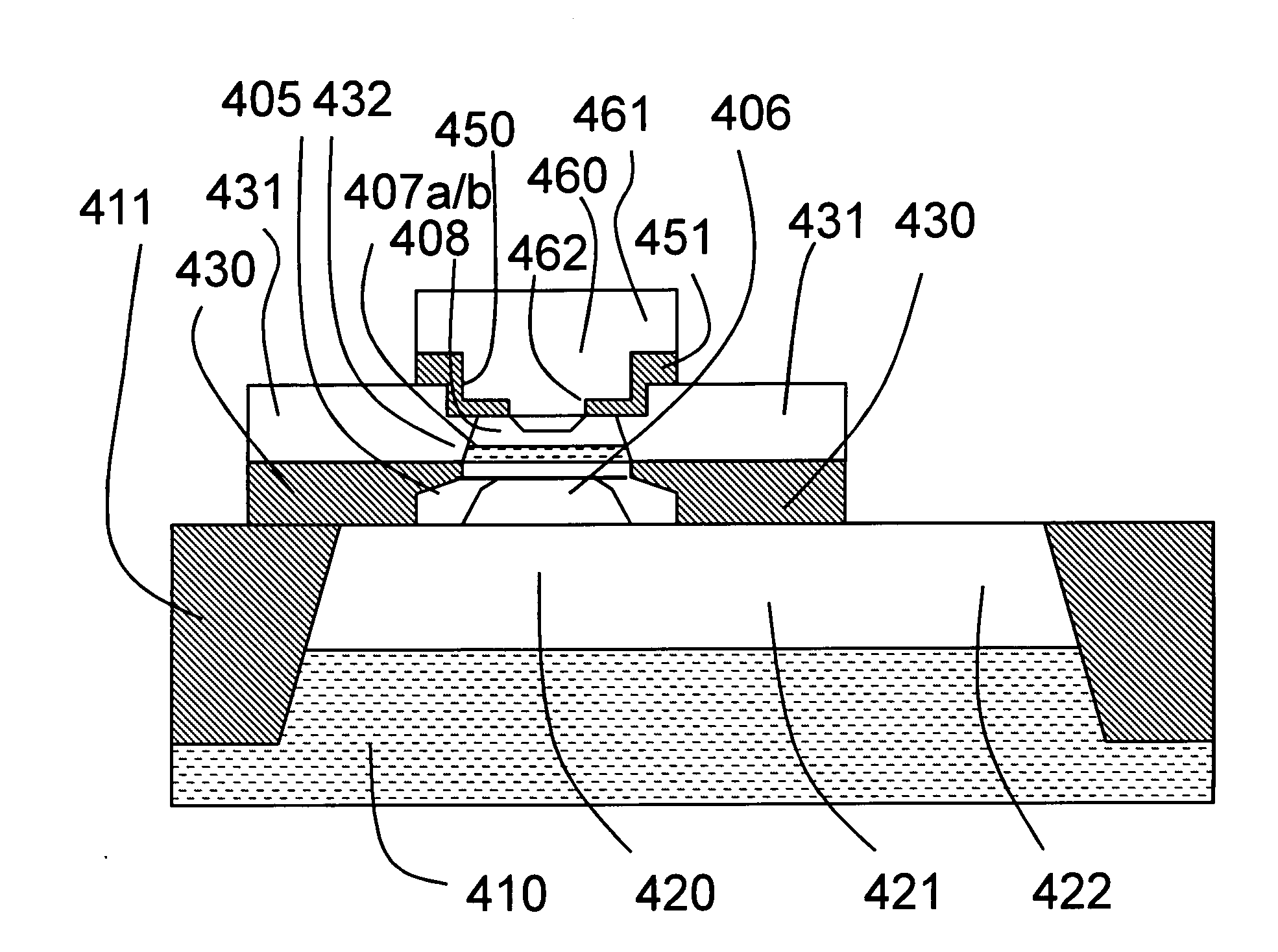
[0102]A first embodiment of a semiconductor device comprising a vertical bipolar transistor, in which the overlap between the emitter contact and the base connection region is produced self-aligningly with respect to the emitter window, shall now be described with reference to FIG. 5, which shows a cross-sectional view of this first embodiment.

[0103]In this example, a vertical NPN bipolar transistor is produced on a high-impedance, monocrystalline P conductive type Si substrate 410. However, the arrangement described here is not limited to P conductive type Si substrates. The essential features can also be applied to substrates of the opposite conductivity type. CMOS transistors may also be simultaneously present on substrate 410, but are not shown in FIG. 5.

[0104]The vertical NPN bipolar transistor shown in FIG. 5 comprises an N conductive type lower collector region 420, which forms a first vertical portion of a collector of the bipolar transistor, and a likewise N conductive type...

example 2

[0139]A second embodiment of a semiconductor device according to the invention, comprising a vertical bipolar transistor in which the overlap between the emitter contact and the base connection region is produced self-aligningly, and in which the base connection region consisting of a different material from that used in the inner transistor may be wholly or partially monocrystalline, shall now be described with reference to FIG. 13 and FIG. 21. FIG. 13 shows a cross-sectional view of this second embodiment. FIG. 21 shows a variant of the second embodiment. In FIGS. 13 to 21, which pertain to the two variants of Example 2, the same reference signs are used for the same structural elements as in Example 1 and FIGS. 5 to 12.

[0140]The structure of the vertical bipolar transistor in this second embodiment is identical in many respects and in both variants to that of the first embodiments, with the exception of the following structural features:[0141]There is no inner polycrystalline por...


PUM


Abstract

A semiconductor device, comprising a substrate layer made of a semiconductor material of a first conductivity type and having a first insulation region, and a vertical bipolar transistor having a first vertical portion of a collector made of monocrystalline semiconductor material of a second conductivity type and disposed in an opening of the first insulation region, a second insulation region lying partly on the first vertical portion of the collector and partly on the first insulation region and having an opening in the region of the collector, in which opening a second vertical portion of the collector made of monocrystalline material is disposed, said portion including an inner region of the second conductivity type, a base made of monocrystalline semiconductor material of the first conductivity type, a base connection region surrounding the base in the lateral direction, a T-shaped emitter made of semiconductor material of the second conductivity type and overlapping the base connection region, wherein the base connection region, aside from a seeding layer adjacent the substrate or a metallization layer adjacent a base contact, consists of a semiconductor material which differs in its chemical composition from the semiconductor material of the collector, the base and the emitter and in which the majority charge carriers of the first conductivity type have greater mobility compared thereto.

Description

CROSS REFERENCE TO RELATED APPLICATIONS[0001]This application is the U.S. National Stage of International Application No. PCT / EP2009 / 066316 filed on Dec. 3, 2009 which was published in German on Jun. 17, 2010 under International Publication Number WO 2010 / 066630.BACKGROUND OF THE INVENTION[0002]1. Technical Field[0003]The invention relates to a bipolar semiconductor memory device comprising one or more vertical bipolar transistors which have an emitter region, a base region and a collector region, wherein the emitter in standard T-shaped design laterally overlaps the base connection region laterally adjoining the base. The invention also relates to a method for producing such a bipolar semiconductor device.[0004]2. Discussion of Related Art[0005]The performance of silicon-based bipolar transistors (or bipolar junction transistors (BJT)) has been significantly improved in the field of high-speed semiconductors by novel component designs and material components, and by reductions in t...

Claims


Application Information

Patent Timeline
Patent Type & Authority Applications(United States)
IPC IPC(8): H01L29/70H01L21/331
CPCH01L29/0804H01L29/1004H01L29/161H01L29/0821H01L29/66272H01L29/7322H01L29/7371H01L29/66242H01L21/8249H01L21/8222H01L29/0817
Inventor FOX, ALEXANDERHEINEMANN, BERNDMARSCHMEYER, STEFFEN
Owner IHP GMBH INNOVATIONS FOR HIGH PERFORMANCE MICROELECTRONICS LEIBNIZ INST FUR INNOVATIVE
Why Eureka
Try Eureka