Loss modulated silicon evanescent lasers

Active Publication Date: 2012-01-05
RGT UNIV OF CALIFORNIA
View PDF11 Cites 64 Cited by
  • Summary
  • Abstract
  • Description
  • Claims
  • Application Information

AI Technical Summary

Benefits of technology

[0012]To minimize the limitations in the prior art, and to minimize other limitations that will become apparent upon reading and understan

Problems solved by technology

III-V material-based devices are difficult to integrate with electronic devices fabricated on silicon because of lattice mismatches and incompatible crystalline structures between silicon and III-V materials.
Such materials are typically used because Silicon (Si), typically used for electronic communication systems, has an indirect bandgap which makes silicon a poor photon (light) emitter, and thus silicon does not perform well in optical transmitter applications.
The indirect bandgap and resultant poor light emission of silicon has limited the realization of an electrically pumped Si-based laser, which is one of the key elements for optical transmitters and Si-based optical communications systems.
Direct modulation of the injected pump current is a simple approach to such a problem, however, as the injection current is increased, the extinction ratio decrea

Method used


Image

  • Loss modulated silicon evanescent lasers
  • Loss modulated silicon evanescent lasers
  • Loss modulated silicon evanescent lasers

Examples


Embodiment Construction

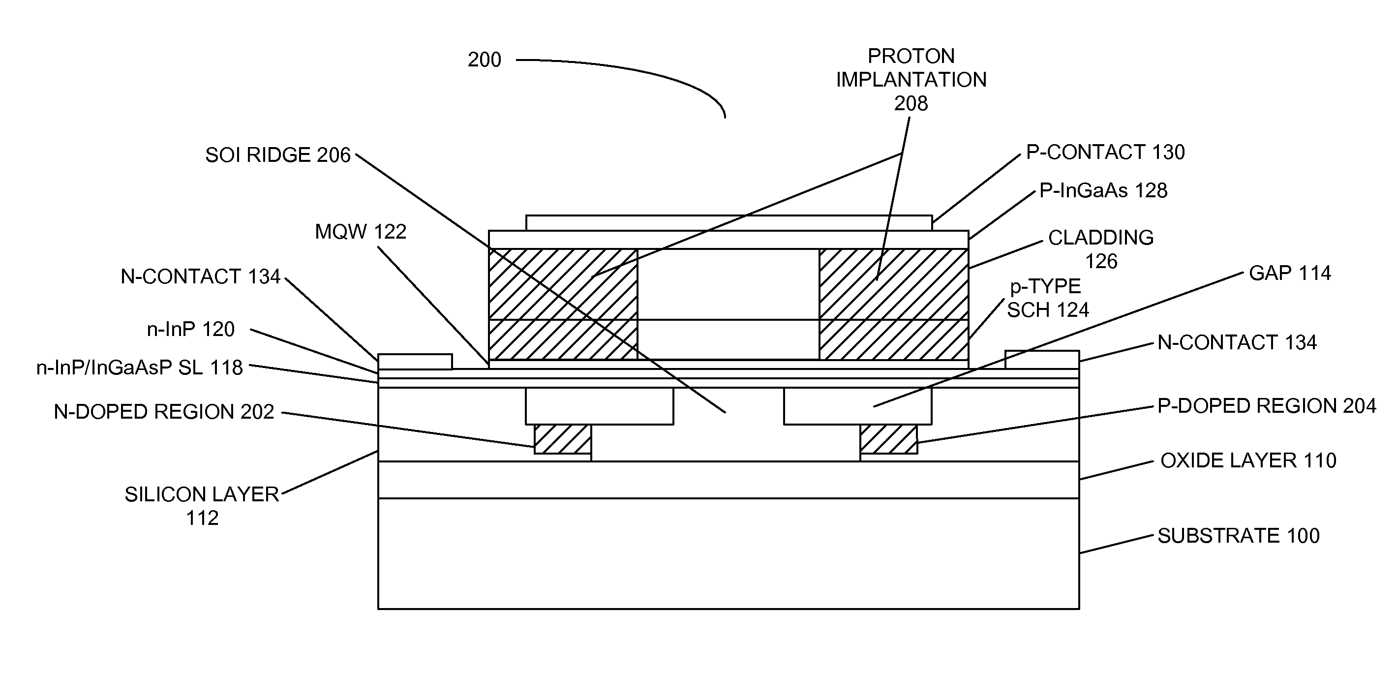
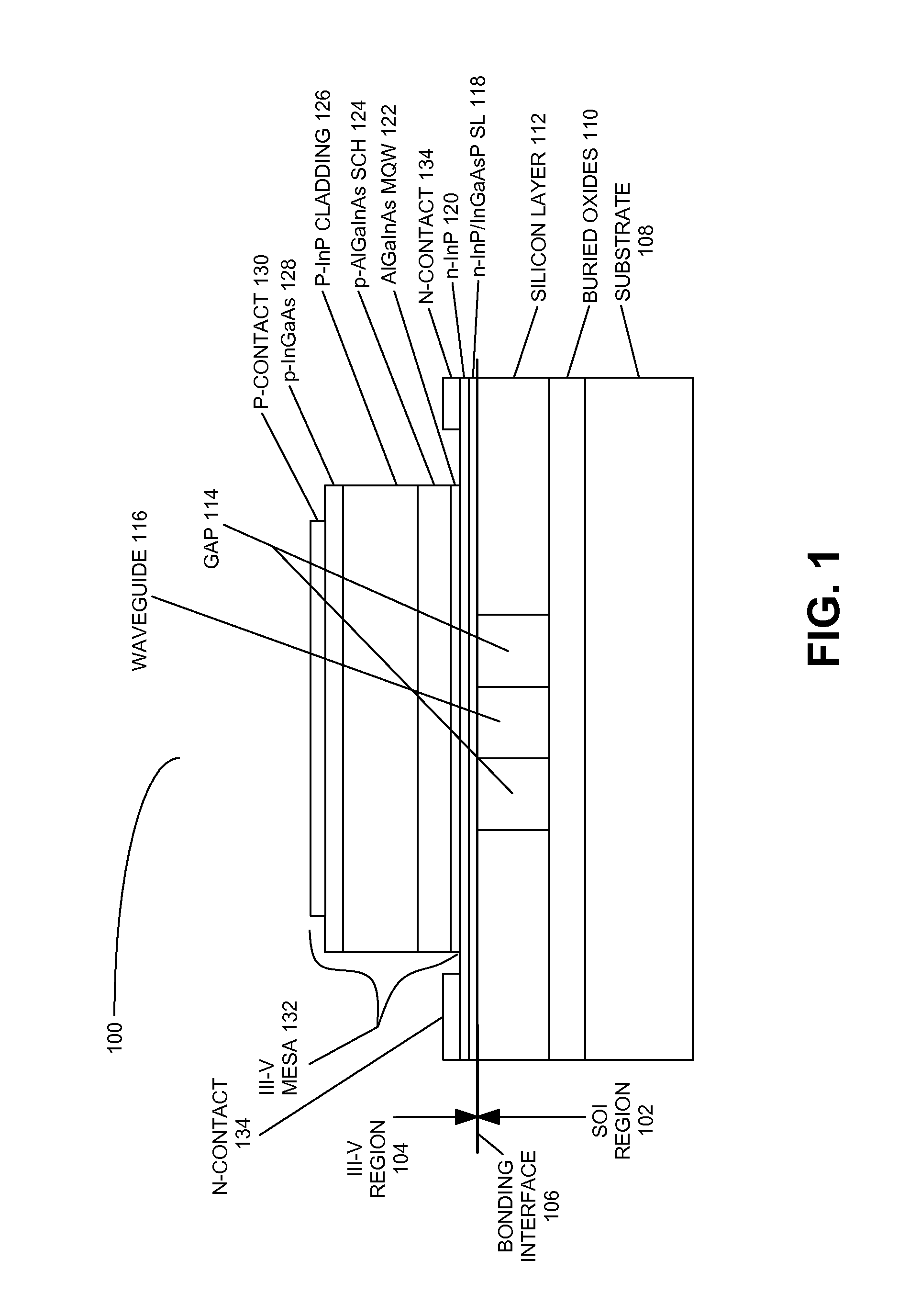
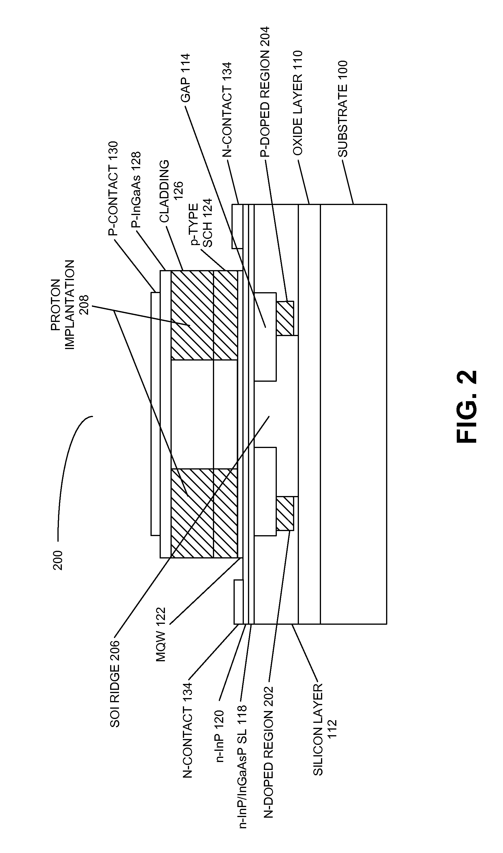
[0032]In the following description, reference is made to the accompanying drawings which form a part hereof, and which is shown, by way of illustration, several embodiments of the present invention. It is understood that other embodiments may be utilized and structural changes may be made without departing from the scope of the present invention.

[0033]Overview

[0034]The present invention describes direct modulation of a hybrid silicon evanescent laser. Rather than change the current to the laser, the present invention keeps the current at a relatively fixed amount, and the loss of the cavity is modulated. Such an approach allows for faster modulation of the output, as well as allowing for control of laser output illumination uniformity (also known as “pattern effects”) and changes in laser output frequency (“chirp”) in the laser outputs.

[0035]Within the loss modulation approach of the present invention, the gain and / or injected current can also be varied to compensate the output to a...


PUM


Abstract

Loss modulated silicon evanescent lasers are disclosed. A loss-modulated semiconductor laser device in accordance with one or more embodiments of the present invention comprises a semiconductor-on-insulator (SOI) structure resident on a first substrate, the SOI structure comprising a waveguide in a semiconductor layer of the SOI structure, and a semiconductor structure bonded to the semiconductor layer of the SOI structure, wherein at least one region in the semiconductor layer of the SOI structure controls a photon lifetime in the semiconductor laser device.

Description

STATEMENT REGARDING FEDERALLY SPONSORED RESEARCH OR DEVELOPMENT[0001]This invention was made with Government support under Grant No. 482530-25615, awarded by DARPA. The Government has certain rights in this invention.BACKGROUND OF THE INVENTION[0002]1. Field of the Invention[0003]The present invention relates generally to semiconductor devices, and, more specifically, to loss modulated silicon evanescent lasers.[0004]2. Description of the Related Art[0005]Semiconductor chip level bonded devices have found uses in several consumer and commercial applications. Typically, semiconductor devices are made from a single type of material, or different types of material are grown onto a substrate based on lattice matching and compatible crystalline structures. As such, devices manufactured from semiconductor materials from Groups III and V of the periodic table materials) are typically grown on gallium arsenide or other compound semiconductor substrates, while silicon devices are grown or fa...

Claims


Application Information

Patent Timeline
IPC IPC(8): H01S5/323H01L21/02
CPCH01S5/021H01S5/0265H01S5/14H01S5/1032H01S5/1071H01S5/06226H01S5/06H01S5/10
Inventor BOWERS, JOHN E.DAI, DAOXIN
Owner RGT UNIV OF CALIFORNIA
Why Eureka
Try Eureka