Low power static random access memory

a static random access and low power technology, applied in static storage, information storage, digital storage, etc., can solve the problems of half-selected cells flipping, low cell array supply voltage aggravated, and failure of cell stability to limit read v, so as to improve the switching speed of cell array supply, improve the switching power and noise, and improve the effect of cell supply switching speed

Active Publication Date: 2012-01-12
FARADAY TECH CORP +1
View PDF12 Cites 26 Cited by
  • Summary
  • Abstract
  • Description
  • Claims
  • Application Information

AI Technical Summary

Benefits of technology

[0007]Accordingly, one objective of the present invention is to provide a SRAM that can keep the cell array supply voltage at low level during Write operation to facilitate writing of data into the memory cell and to minimize power consumption in Write mode. Also, the cell array supply for the SRAM is raised only during Read operation to maintain adequate RSNM. The SRAM maintains low voltage in Write mode, which cannot be achieved using conventional 6T SRAM, to achieve Ultra-Low-Power (herein after ULP) mode of operation.
[0008]Another objective of the present invention is to provide a SRAM that can keep the cell array supply voltage at low level during Write operation to facilitate writing of data into the memory cell and to minimize power consumption in Write mode. Also, the cell array supply for the SRAM is raised only for the selected columns during Read operation to maintain adequate RSNM and to minimize power consumption in Read mode. The SRAM maintains low voltage for unselected columns in Read mode, and raises only the cell supply voltage for the selected columns in Read mode, thus achieving the Absolutely-Lowest-Power (herein after ALP) mode of operation.
[0011]Moreover, via aforementioned embodiments, only the cell array supply for one side of the cell (i.e. half-cell)is raised in Read mode, such that the cell supply switching power and noise can be reduced and the cell supply switching speed improved. Furthermore, in the ALP mode, only the cell array supply of the selected columns will be switched, thus the switching power and noise are further reduced, and the cell array supply switching speed further improved. Besides, only simple control circuit structure is needed. For example, each column only needs a power-switch device and power-keeping (keeper)devices. Also, to operate in the ALP mode, only simple decoding logic circuit is needed. Therefore, the device and area overhead is quite small.

Problems solved by technology

This Read disturb voltage degrades the Read Static Noise Margin (herein after RSNM) and may cause cell stability failures to limit the Read Vmin (Minimum operating voltage).
However, low cell array supply voltage aggravates the “Half-Select disturb”, and the half-selected cells may flip.
As a result, the cell array supply voltage for the entire active bank needs to be raised to higher voltage level, thus causing more power consumption.

Method used


Image

  • Low power static random access memory
  • Low power static random access memory
  • Low power static random access memory

Examples


Embodiment Construction

[0026]Certain terms are used throughout the description and following claims to refer to particular components. As one skilled in the art will appreciate, electronic equipment manufacturers may refer to a component by different names. This document does not intend to distinguish between components that differ in name but not function. In the following description and in the claims, the terms “include” and “comprise” are used in an open-ended fashion, and thus should be interpreted to mean “include, but not limited to . . . ”. Also, the term “couple” is intended to mean either an indirect or direct electrical connection. Accordingly, if one device is coupled to another device, that connection may be through a direct electrical connection, or through an indirect electrical connection via other devices and connections.

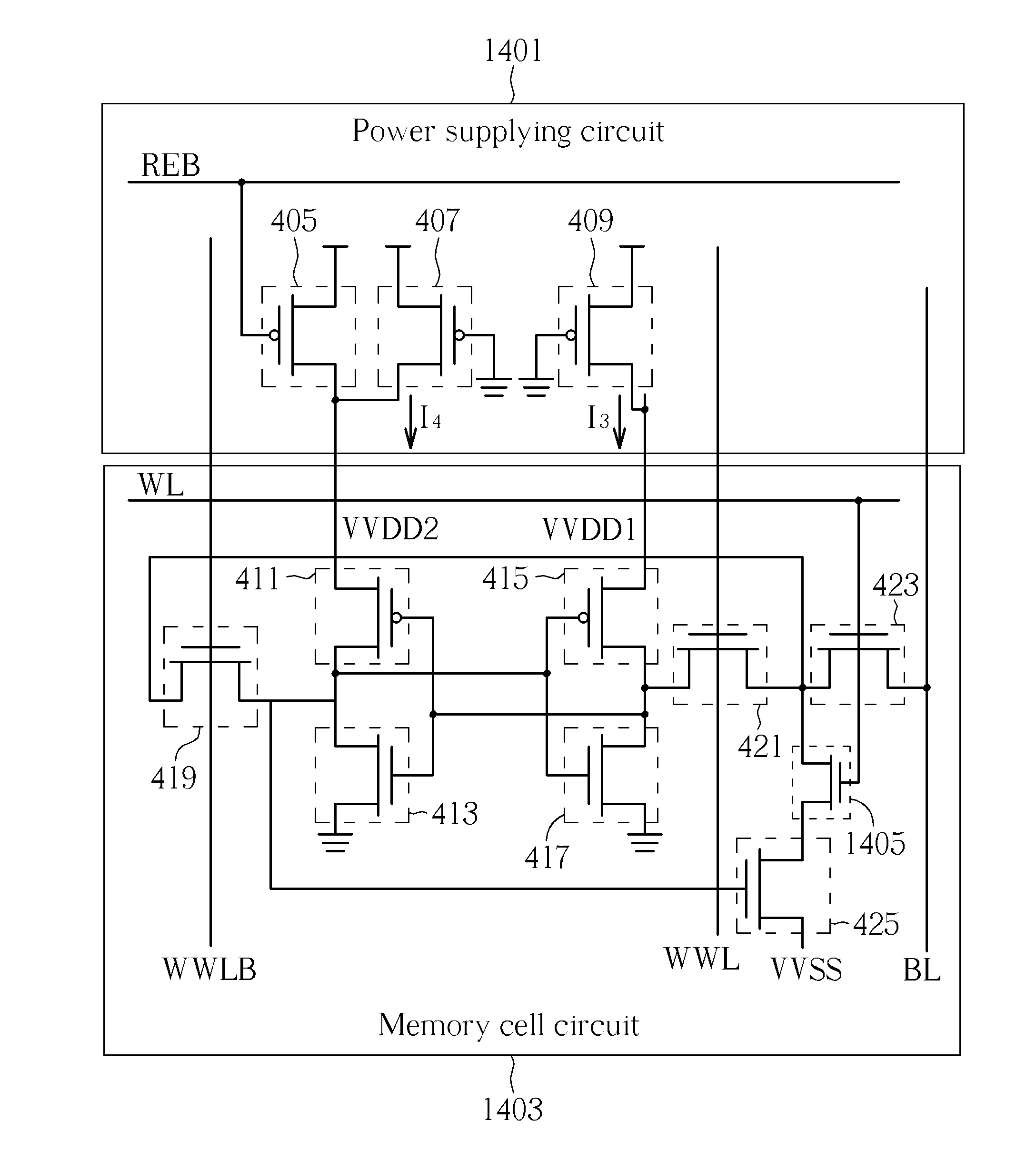
[0027]According to the concept disclosed in present application, two modes of the memory cell circuit are provided. One is called ULP mode and the other one is called ALP...


PUM


Abstract

A SRAM that keeps the memory cell array under a low voltage in the Standby mode and Write mode, and raises the memory cell array supply voltage to a high voltage in the Read mode. A SRAM comprising: at least one memory cell circuit, comprising a latch circuit with at least two inverters, and comprising two power receiving terminals for receiving power; and a power supplying circuit, for providing the power to the memory cell circuit, such that the voltages at the power receiving terminals of the latch circuit is below a predetermined voltage level when data is written to the latch circuit. In one embodiment, the memory cell circuit includes a plurality of data accessing terminals and the data accessing terminals are respectively controlled by at least two pass-transistor switch devices.

Description

CROSS REFERENCE TO RELATED APPLICATIONS [0001]This application claims the provisional application, which is U.S. Provisional Application No. 61 / 361,528, filed Jul. 6, 2010 and is included herein by reference.BACKGROUND OF THE INVENTION[0002]1. Field of the Invention[0003]The present invention relates to a static random access memory (SRAM), and particularly relates to a SRAM that keeps the memory cell array under a low voltage in the Standby mode and Write mode, and raises the memory cell array supply voltage to a high voltage in the Read mode.[0004]2. Description of the Prior Art[0005]FIG. 1 is a circuit diagram illustrating a related prior art 6T SRAM static random access memory structure. As shown in FIG. 1, the 6T SRAM structure has a plurality of memory cell circuits, but only two memory cell circuits 101, 103 are symbolized for explaining. For a 6T SRAM cell during Read operation (FIG. 2), a Read disturb voltage is generated at the cell “0” storage node (NT in FIG. 2) when the...

Claims


Application Information

Patent Timeline
Patent Type & Authority Applications(United States)
IPC IPC(8): G11C5/14
CPCG11C11/413G11C11/417
Inventor CHUANG, CHING-TEYANG, HAO-IHSIA, MAO-CHIHHWANG, WEICHEN, CHIA-CHENGSHIH, WEI-CHIANG
Owner FARADAY TECH CORP
Why Eureka
Try Eureka