

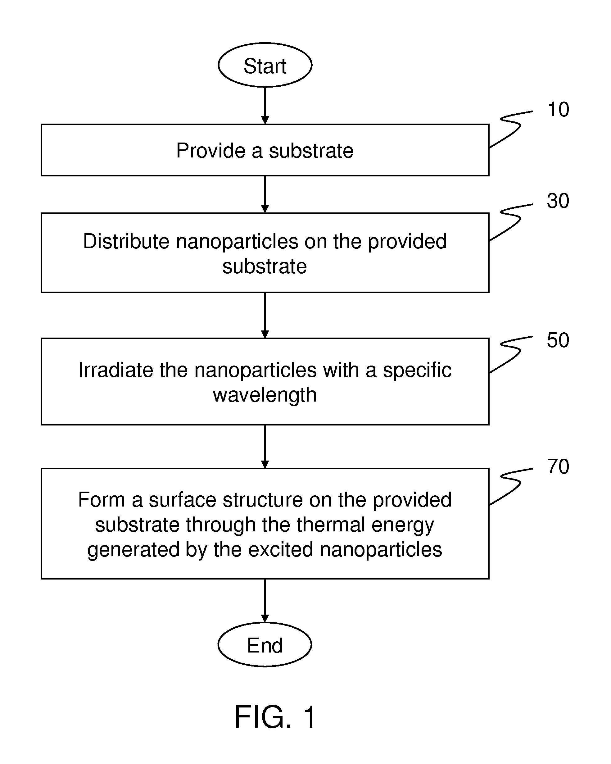
Method for manufacturing a substrate with surface structure by employing photothermal effect
a surface structure and photothermal effect technology, applied in the direction of photomechanical equipment, instruments, dielectric characteristics, etc., can solve the problems of high cost of fabricating micro/nano structure using these technologies, difficult to manufacture micro/nano structure surface in large area, complex fabrication process, etc., to achieve the effect of reducing residual stress, simple and cheaper fabricated process, and reducing manufacturing cos
- Summary
- Abstract
- Description
- Claims
- Application Information
AI Technical Summary
Benefits of technology
Problems solved by technology
Method used
Image

Examples
example 1
[0096]The Au-nanoparticles (i.e., the nanoparticle was made of Au) with a particle size of about 20 nm were fixed on a transparent substrate, and then placed on a surface of a substrate made of a polymer material. The Au-nanoparticles closely contacted the surface of the substrate. Then, the green laser with a wavelength of 532 nm was used to irradiate the transparent substrate with Au-nanoparticles for about 15 seconds. The Au-nanoparticles were excited on the substrate. At this time, the Au-nanoparticles generated temperature of up to 200° C. within 15 seconds upon being irradiated by the green laser. After exposed time, i.e. the time of irradiation, of 15 seconds, the transparent substrate and the Au-nanoparticles were removed from the substrate to obtain the substrate with pores. Before being irradiated by the green laser, the surface of the substrate having the Au-nanoparticles was observed with an atomic force microcopy (AFM), as shown in FIG. 9A. After being irradiated by the...
example 2
[0099]The green laser with a wavelength of 532 nm and a power of 100 mW was used to irradiate the Au-nanoparticles where was placed on the substrate 1 through the transparent substrate for about 10 minutes. Once the irradiation was completed, the transparent substrate and Au-nanoparticles were removed, so as to obtain the substrate 1′. Before being irradiated by the green laser, the substrate having the Au-nanoparticles was observed with an AFM, as shown in FIG. 11A. After being irradiated by the green laser, the substrate 1′ obtained was observed with an AFM, as shown in FIG. 11B.
example 3
[0100]The green laser with a wavelength of 514.5 nm and a power of 1 W irradiated the Au-nanoparticles placed on the substrate 2 through the transparent substrate for about 20 minutes. Once the irradiation was completed, the transparent substrate and Au-nanoparticles were removed, so as to obtain the substrate 2′. Before being irradiated by the green laser, the substrate having the Au-nanoparticles was observed with an AFM, as shown in FIG. 12A. After being irradiated by the green laser, the obtained substrate 2′ was observed with an AFM, as shown in FIG. 12B.
PUM
| Property | Measurement | Unit |
|---|---|---|
| specific wavelength | aaaaa | aaaaa |
| particle size | aaaaa | aaaaa |
| particle size | aaaaa | aaaaa |
Abstract
Description
Claims
Application Information