Fuse element

a technology of fuse element and element, applied in the field of fuse element, can solve the problems of material loss, different temperature expansion coefficient, material material damage, etc., and achieve the effect of preventing inflammation

Active Publication Date: 2012-01-19
SCHURTER
View PDF43 Cites 13 Cited by
  • Summary
  • Abstract
  • Description
  • Claims
  • Application Information

AI Technical Summary

Benefits of technology

[0011]The advantage of the embodiment according to the invention is essentially that a stable insulation strength of the fuse is ensured at the highest possible ambient temperatures for electric and / or electronic circuits, and it has a current-time behavior that is distinguished highly positively over the previous versions offered in the prior art for making fuses, and moreover the material and production costs can be reduced considerably compared to the typical fuses known from the prior art.
[0016]As noted at the outset, the temperature stability, or a better term for it is temperature resistance, of the fuse element is an essential factor for being suitable to be capable of being made integrally with the printed circuit board, or in other words, during the same process as the production of the printed circuit board. If a classically constructed printed circuit board substrate is used, and the actual fuse element is formed from the metal or metal alloy lining it, then he fuse element has one side virtually free, so that the fuse element can in this way dissipate heat to the surroundings. However, if the fuse is used in a multilayer system comprising a plurality of printed circuit board substrates resting on one another, then the actual fuse element, which is also somewhat vaguely called a melting conductor, is embedded or laminated completely in the aforementioned multilayer system. As a result, the heat dissipation of the fuse element because of its heating is consequently more greatly hindered by the currents that flow through the fuse element.
[0018]By utilizing this advantageous principle to create an unhindered heat dissipation of the actual fuse element, it can furthermore be advantageous in the vicinity of the site of a printed circuit board substrate on which the fuse (12) is provided in the metal or the metal alloy (15), for one void each to be provided in the second printed circuit board substrate resting adjacent to the first printed circuit board substrate and in the vicinity of the site of the first printed circuit board substrate on which the fuse is provided, the voids being in the form of respective recesses. This has the extraordinary advantage that in fact, the fuse element (melting conductor) is provided with an adjacent void on both of its sides in the multilayer substrate, so that the heat produced by a high current flow through the fuse element can be dissipated to both sides.
[0021]However, for certain applications it can also be advantageous to close off the void or voids with a layer on the side facing away from the fuse element.
[0022]This layer can perform multiple tasks; for instance, it can prevent an electric arc or molten components of the fuse from escaping to the surroundings from the immediate vicinity of the fuse, and it is equally capable, upon the occurrence of an electric arc, of preventing the escape of the electric arc from the void to the surroundings.
[0024]Although the membrane should permit an air exchange into the void and out of the void, it also should prevent molten components of the fuse from being able to escape from the void and also should prevent components adjacent to the fuse element and the multilayer system overall from bursting into flame.

Problems solved by technology

One essential problem in the embodiment of fuse elements in the case of the metals or metal alloys, such as copper or copper alloys, that are laminated onto the printed circuit board substrate, is that the actual printed circuit board material that the printed circuit board substrate comprises, which as a rule is epoxy resin-reinforced, woven glass fabric, has a different temperature expansion coefficient from the material of the conductors, such as copper, for instance.
One disadvantage of the known printed circuit board substrates or printed circuit board material that until now has generally been used for producing printed circuit boards assembled with electric and electronic components is that the operating temperatures of printed circuit board materials thus far typically allow temperatures only below 200° C., because higher operating temperatures damage the printed circuit board substrate material.
As a consequence of high temperatures, this material loses strength, and delamination and finally decomposition and carbonization of the polymer ensue.
The result is conductive, relatively low-impedance layers, the disadvantageous consequence of which is that the minimum requisite insulation resistances of fuses and fuse elements constructed in this way fail to be attained.
In another type of fuse known in the prior art, an Al2O3 ceramic, which even at very much higher temperatures are stable as fuses on the basis of the above-described printed circuit board substrate material, serves as a basis; however, these fuses on Al2O3 ceramic have a temperature expansion coefficient that as a rule is below 8 ppm / K, which in turn also has an adverse effect on the stability of the fuse and thus of the entire electric and / or electronic circuit, since between the actual printed circuit board substrate material and the ceramic, stresses arise that cause cracks in the ceramic and damage it, making it unusable.

Method used


Image

  • Fuse element
  • Fuse element
  • Fuse element

Examples


first embodiment

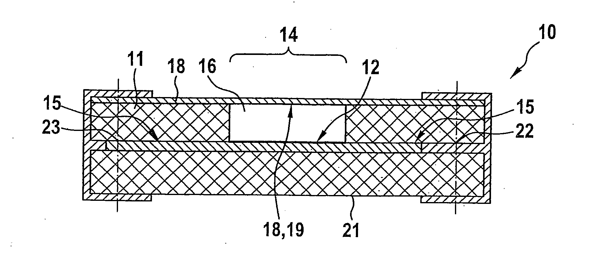
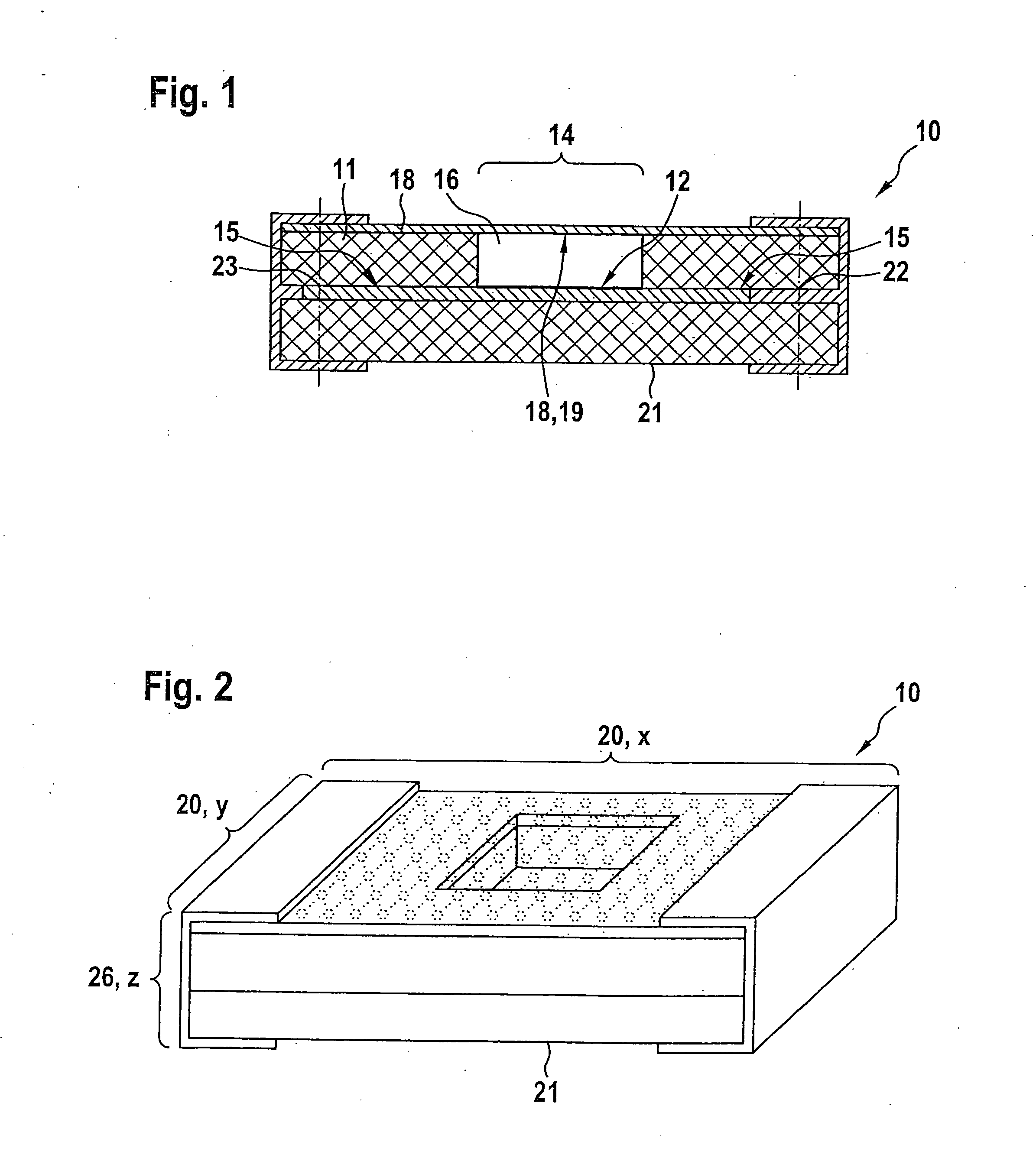
[0037]First, to the views in FIGS. 1 and 2 will be discussed, in which a fuse element 10 of the invention is shown.

[0038]FIGS. 1 and 2 pertain to the fuse element 10, in which the fuse 12 of the invention is provided on a printed circuit board substrate or printed circuit board substrate material 11. The fuse 12 is provided on the printed circuit board substrate 11, which is coated in a known manner with a metal or metal alloy 12 by a coating procedure, and the fuse 12 is generated by means of photolithographic and / or printing image-producing techniques, such as screen printing, and ensuing etching or engraving processes, as is generally done to make printed circuit boards with conductor tracks that are to be provided on the printed circuit boards. Both conventionally constructed printed circuit board substrates with one- and / or two-sided coating with metal or metal alloys and the known printed circuit board substrates that are formed by the multilayer technology or used for it, are...

second embodiment

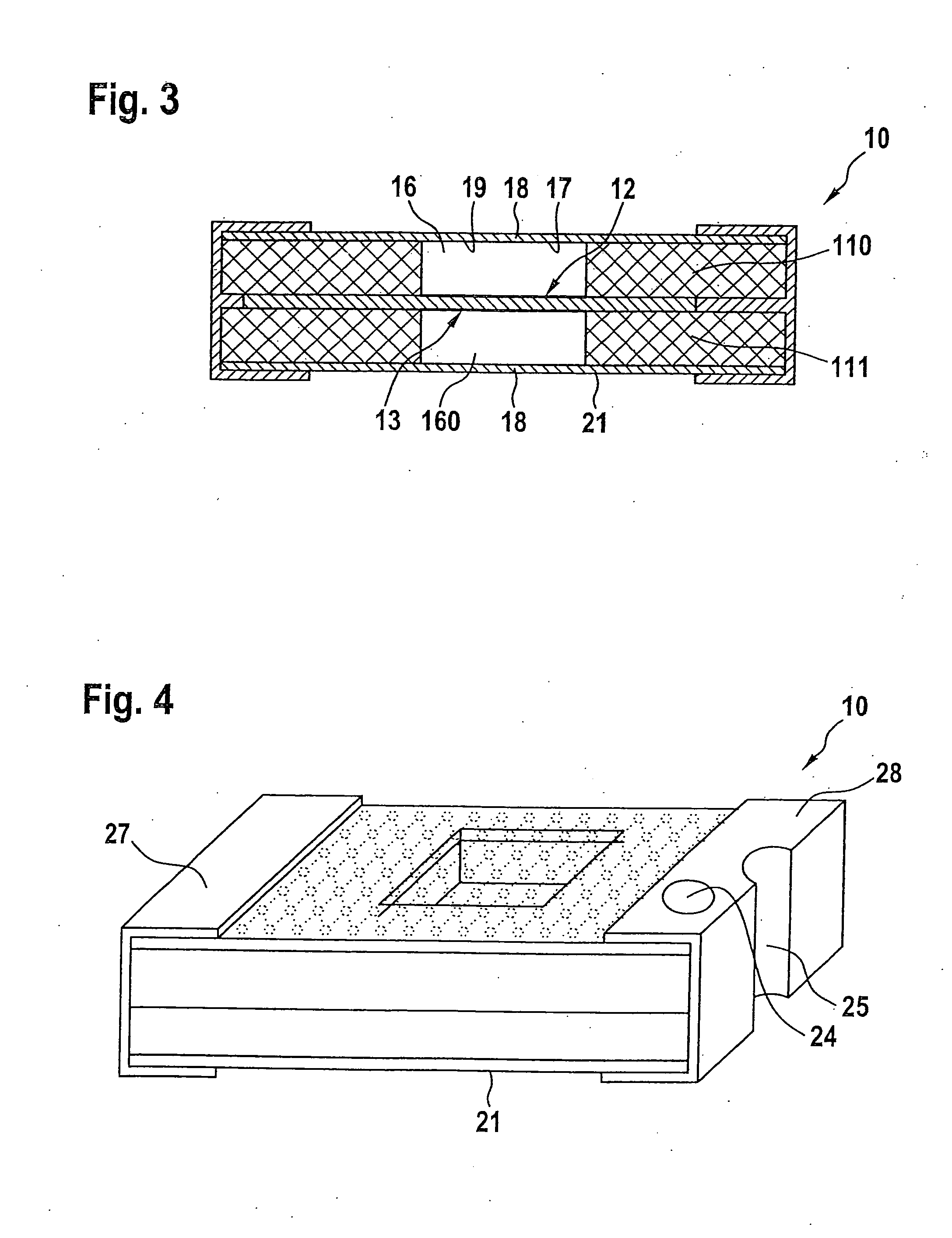
[0042]In the vicinity of the fuse 12, the printed circuit board substrate 11, and this applies equally to the printed circuit board substrates 110, 111 that will be described below in conjunction with the fuse element shown in FIGS. 3 and 4, through-holes not shown here can be formed, which can be created for instance by means of laser devices, by means of which the characteristic time-current curve of the fuse 12 can be designed as faster-acting or slower-acting, and the current-time integral can also be varied by means of this provision. It is equally possible for the metal or metal alloy that forms the melting part of the fuse to have a plurality of such through-holes, so that by that means as well, either alternatively or in addition, it is possible to vary the aforementioned parameters. The void 16 and / or the void 16, 160 of the embodiment of the fuse element 10 of FIGS. 3 and 4 can be filled at least in part by an insulating means, not shown here; this insulating means can for...


PUM

PropertyMeasurementUnit
temperaturesaaaaaaaaaa
operating temperaturesaaaaaaaaaa
temperatureaaaaaaaaaa

Abstract

A fuse element (10), in particular suited for use in electric and / or electronic circuits constructed by multilayer technology, including a printed circuit board substrate material (11), which is usable particularly in the multilayer technology and is coated with a metal or metal alloy (15), from which metal or metal alloy the fuse (12) is generated by means of photolithographic and / or printing image-producing techniques and ensuing etching or engraving processes, is proposed. The fuse (10) is distinguished in that the printed circuit board substrate material (11), on which the fuse (12) can be provided, includes at least a high-temperature-stable, electrically insulating material, with a coefficient of thermal expansion that varies essentially analogously to the coefficient of thermal expansion of the metal or metal alloy (15) from which the fuse (12) is made.

Description

BACKGROUND OF THE INVENTION[0001]1. Field of the Invention[0002]The invention relates to a fuse element, in particular suited for use in electric and / or electronic circuits constructed by multilayer technology, including a printed circuit board material, which is usable particularly in the multilayer technology and is coated with a metal or metal alloy, from which metal or metal alloy the fuse is generated by means of photolithographic and / or printed image-producing techniques and ensuing etching or engraving processes.[0003]2. Related Art[0004]Circuit boards of the kind used in the manufacture of both electronic and electric circuits, whether with the classical one- or two-sided coating with conductive materials for forming conductor tracks, but also in what is known as the multilayer technology, in which printed circuit boards formed in many layers are used, are assembled with all conceivable kinds of active and passive electronic and electric components, and this assembly is toda...

Claims


Application Information

Patent Timeline
Patent Type & Authority Applications(United States)
IPC IPC(8): H01H85/046
CPCH01H69/022H01H85/046H05K2201/10181H05K2201/0187H05K1/0293H05K1/0373H05K2201/0209H05K1/02H01H85/0241H01H2085/0275
Inventor BLATTLER, HANS-PETERSTRAUB, PETERRAMOS, JOSE
Owner SCHURTER
Why Eureka
Try Eureka