Impedance matching device

a technology of impedance matching and matching circuit, which is applied in the direction of fixed inductance, inductance, electrical equipment, etc., can solve the problems of increasing production cost, complicating manufacturing process, and requiring small impedance matching circuit size, and achieve large current tolerance and small variation in quality

a technology of impedance matching and matching circuit, which is applied in the direction of fixed inductance, inductance, electrical equipment, etc., can solve the problems of increasing production cost, complicating manufacturing process, and requiring small impedance matching circuit size, and achieve large current tolerance and small variation in quality

US20120019334A1Inactive Publication Date: 2012-01-26NGK INSULATORS LTD

Image

  • Impedance matching device
  • Impedance matching device
  • Impedance matching device

Examples


example

(1) Explanation Based on an Equivalent Circuit

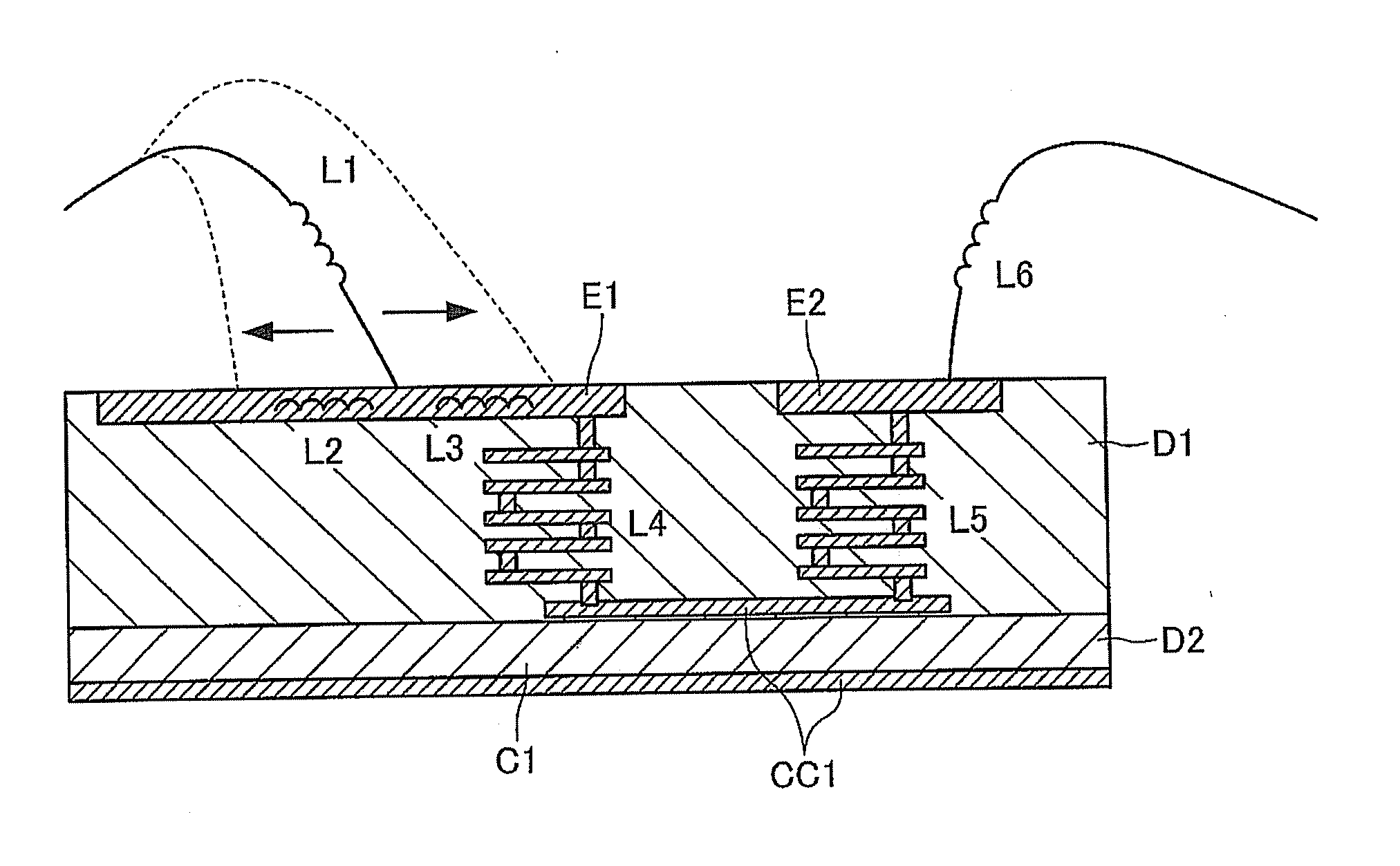
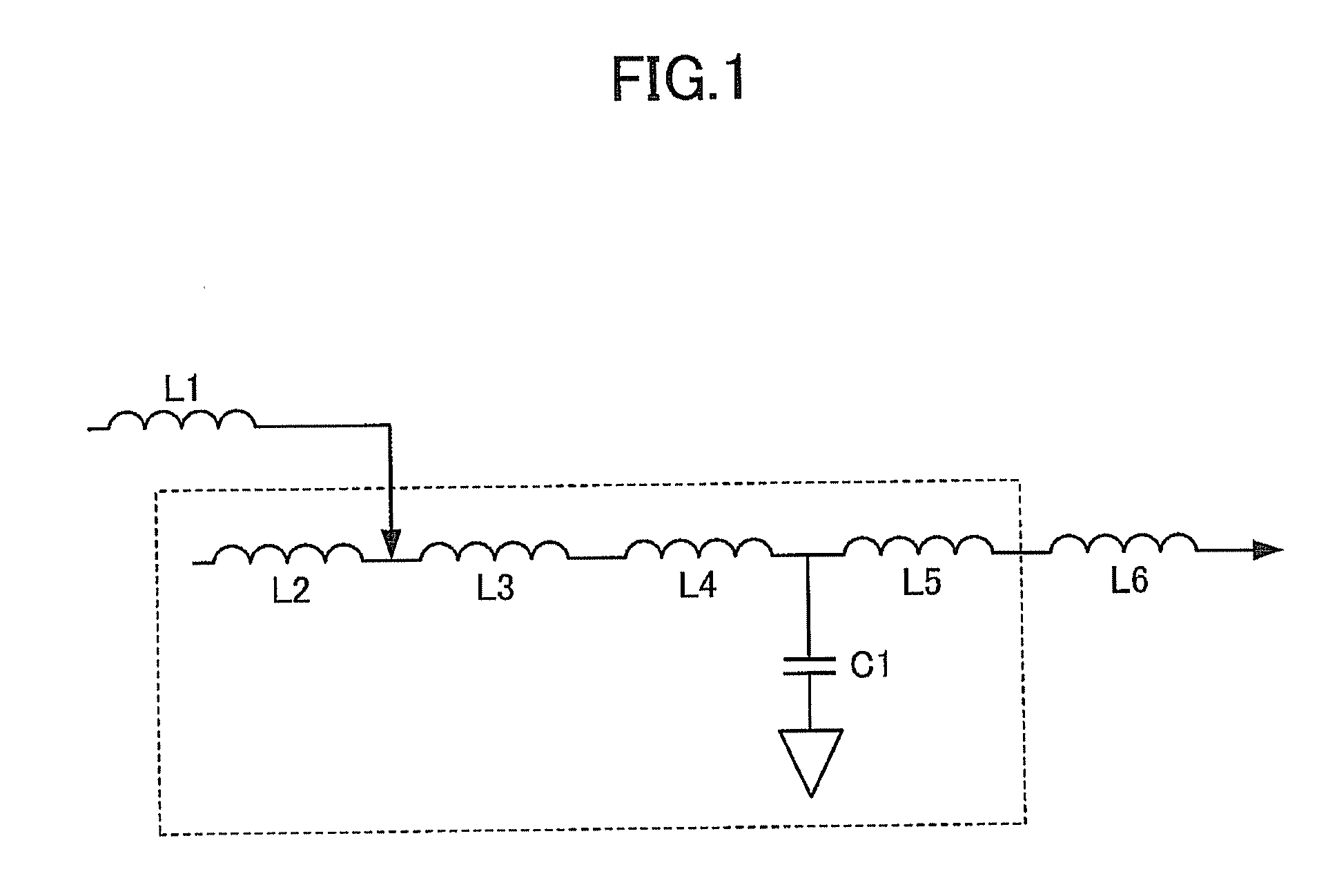
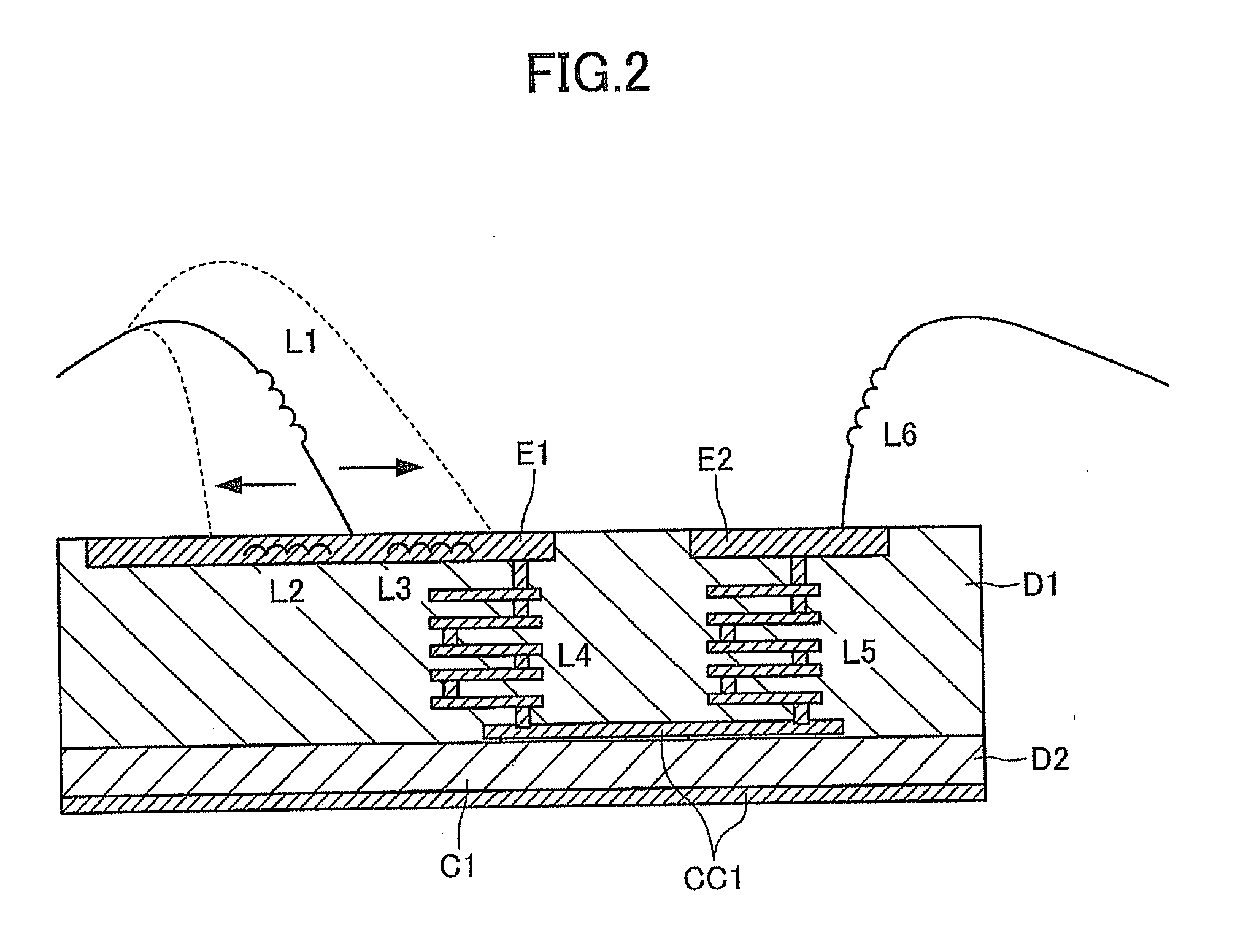
[0111]FIG. 1 is an equivalent circuit schematic showing the configuration of an impedance matching device according to the present example. Components inside the tetragonal frame depicted with dotted line in FIG. 1 represent components included in the impedance matching device according to the present example. Namely, in FIG. 1, L1 and L6 are components not included in the impedance matching device according to the present example, and specifically represent metal wires for connecting the impedance matching device according to the present example and another device (for example, an external circuit such as high frequency wave semiconductor amplifier).

[0112]On the other hand, L4 and L5 represent inductor portions embedded inside the first dielectric material D1 (not shown in FIG. 1) in the impedance matching device according to the present example. To the portion where the inductor portions L4 and L5 are connected, the capacitor portion C...


PUM


Abstract

The present invention intends to provide a small-sized impedance matching device with a small variation in quality and large-current tolerance. The above described intention of the present invention is achieved by an impedance matching device, which comprises a wiring portion comprising a conductor pattern for wiring, embedded inside or formed on the surface of first dielectric material, and either one or both of an inductor portion comprising a conductor pattern for inductor, embedded inside or formed on the surface of the first dielectric material, or a capacitor portion comprising at least one pair of conductor patterns for capacitor and second dielectric material with a dielectric constant larger than that of the first dielectric material, existing between the pair of conductor patterns for capacitor wherein the thicknesses of the conductor pattern for wiring and the conductor pattern for inductor are 20 μm or more.

Description

TECHNICAL FIELD[0001]The present invention relates to an impedance matching device. Specifically, the present invention relates to a small-sized impedance matching device with a small variation in quality and large-current tolerance.BACKGROUND ART[0002]In general, since the output impedance of a semiconductor element consisting of silicon (Si), gallium nitride (GaN) or the like is small, such a semiconductor element is often connected with a circuit for matching impedance when it is connected with an external circuit. Such a semiconductor element is connected with an impedance matching circuit to be capable of matching a characteristic impedance of an external circuit and transmitting the output from the semiconductor element.[0003]The above-described impedance matching circuit is often constituted by a capacitor element and an inductor element consisting of a thin line of conductor connecting the capacitor element and a semiconductor element as described above (for example, metal w...

Claims


Application Information

Patent Timeline
26 Jan 2012
Publication
US20120019334A1
IPC
H03H7/38
CPC
H01F17/02; H03H7/38; H01F2017/0026
Inventors
HIRAI, TAKAMI; NAMERIKAWA, MASAHIKO