Semiconductor device structure and method for fabricating the same

a technology of semiconductor devices and semiconductors, applied in the field of semiconductor devices, can solve the problems of serious distortion of images formed on wafers, approaching the theoretical limit of photolithography systems, and the scale of integrated circuits (ics), and achieve the effect of simplifying the formation of contacts

Active Publication Date: 2012-02-02
INST OF MICROELECTRONICS CHINESE ACAD OF SCI
View PDF3 Cites 38 Cited by
  • Summary
  • Abstract
  • Description
  • Claims
  • Application Information

AI Technical Summary

Benefits of technology

[0012]It is an object of the present invention to provide a semiconductor device structure and a method for fabricating the same, to overcome the problems in the prior art as described above, and especially, to simplify the formation of contacts.

Problems solved by technology

Nowadays, Integrated Circuits (ICs) are increasingly scaled down, and feature sizes thereof are becoming smaller and smaller and thus are approaching the theoretical limit of photolithography systems.
Therefore, there are typically serious distortions in an image formed on a wafer by a photolithography, that is, Optical Proximity Effects (OPEs) occur.
Thus, the sidewall spacers of respective gate patterns on two opposite ends of a cut 1003 may merge with each other, resulting in defects such as voids in the cut 1003.
Thus, the defects such as voids in the cuts 1003 as described above will also cause defects in the formed dielectric layer.
Further, since the etching on the source / drain is deeper while the corresponding opening is relatively small (that is, the width to height ratio is small), various problems, such as under-etching, generating voids in the filled metals, and the like, are likely to occur.
This restricts the selection of manufacture processes and causes greater parasitic resistances as well.

Method used


Image

  • Semiconductor device structure and method for fabricating the same
  • Semiconductor device structure and method for fabricating the same
  • Semiconductor device structure and method for fabricating the same

Examples


first embodiment

A First Embodiment

[0033]Hereinafter, a first embodiment of the present invention is described with reference to FIGS. 4-10.

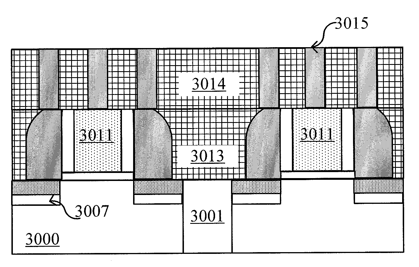
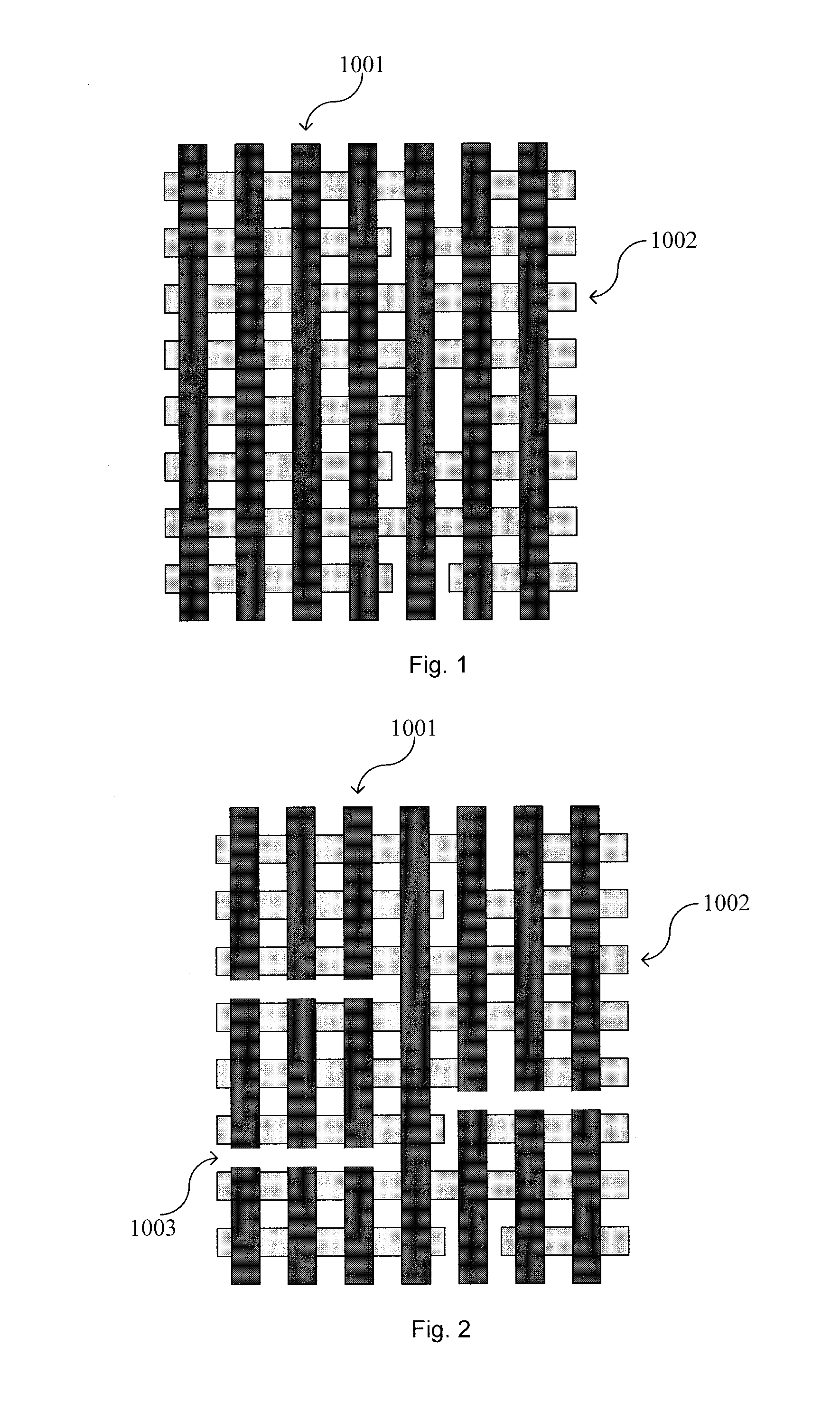
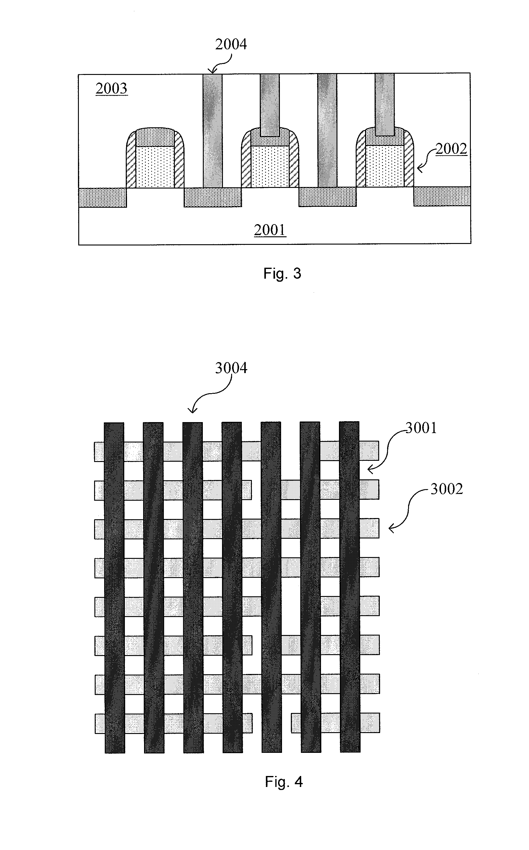
[0034]FIG. 4 shows a part of a layout formed on a semiconductor substrate. Here, the semiconductor substrate may comprise any suitable semiconductor substrate materials, for example, but not limited to, Si, Ge, SiGe, SOI (Silicon on Insulator), SiC, GaAs, or any III-V group compound semiconductor, etc. According to known design requirements (for example, for a p-type substrate or an n-type substrate) in the prior art, the semiconductor substrate 1000 may comprise various doping configurations. Further, the semiconductor substrate 1000 may optionally comprise an epitaxial layer which may be manipulated by stress for performance enhancement.

[0035]In the semiconductor substrate, Shallow Trench Isolations (STIs) 3001 have already been formed, and active regions 3002 are formed in the areas surrounded by STI structures 3001. For of convenience, FIG. 4 only shows stri...

second embodiment

A Second Embodiment

[0057]The method according to the present invention is also compatible with the replacement gate process. Hereinafter, a second embodiment of the present invention is described with reference to FIGS. 11-15, where the replacement gate process in incorporated in this embodiment. The second embodiment differs from the first embodiment mainly in that: a replacement gate process is conducted after the source / drain regions are formed. Specifically, dummy gate lines are firstly formed and then are replaced with replacement gate lines. The same or similar reference numbers in the drawings and in the first embodiment denote corresponding parts.

[0058]In the following, emphasis is given to the differences of the second embodiment from the first embodiment and description of the same processes is omitted. Like reference numbers denote like parts throughout the drawings.

[0059]As shown in FIG. 11(a), dummy gate lines 3005 are formed by printing a pattern of parallel gate lines...


PUM

PropertyMeasurementUnit
distanceaaaaaaaaaa
thicknessaaaaaaaaaa
conductiveaaaaaaaaaa

Abstract

A semiconductor device structure and a method for fabricating the same. A method for fabricating semiconductor device structure includes forming gate lines on a semiconductor substrate; forming gate sidewall spacers surrounding the gate lines; forming respective source/drain regions in the semiconductor substrate and on either side of the respective gate lines; forming conductive sidewall spacers surrounding the gate sidewall spacers; and cutting off the gate lines, the gate sidewall spacers and the conductive sidewall spacers at predetermined positions, in which the cut gate lines are electrically isolated gates, and the cut conductive sidewall spacers are electrically isolated lower contacts. The method is applicable to the manufacture of contacts in integrated circuits.

Description

FIELD OF INVENTION[0001]The present invention relates to the semiconductor field, and more particularly, to a method for fabricating a semiconductor device structure and a resultant semiconductor device structure, where contacts are formed in a self-aligned manner.BACKGROUND[0002]Nowadays, Integrated Circuits (ICs) are increasingly scaled down, and feature sizes thereof are becoming smaller and smaller and thus are approaching the theoretical limit of photolithography systems. Therefore, there are typically serious distortions in an image formed on a wafer by a photolithography, that is, Optical Proximity Effects (OPEs) occur. As the photolithography technology is facing more strict requirements and challenges, there has been proposed the Double Patterning Technology (DPT) which is able to enhance photolithography resolutions. In the DPT, a circuit pattern with a high density is divided into two separate patterns with lower densities, which are then respectively printed onto a targe...

Claims


Application Information

Patent Timeline
Patent Type & Authority Applications(United States)
IPC IPC(8): H01L29/772H01L21/336
CPCH01L21/76897H01L21/823437H01L21/823475H01L29/78H01L27/088H01L29/4983H01L29/66545H01L27/0207
Inventor ZHONG, HUICAILIANG, QINGQINGYIN, HAIZHOU
Owner INST OF MICROELECTRONICS CHINESE ACAD OF SCI
Why Eureka
Try Eureka