

Patternable low-k dielectric interconnect structure with a graded cap layer and method of fabrication
- Summary
- Abstract
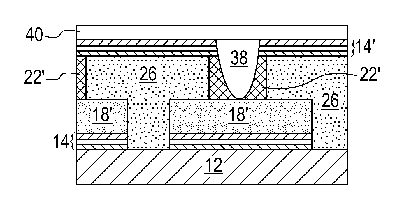
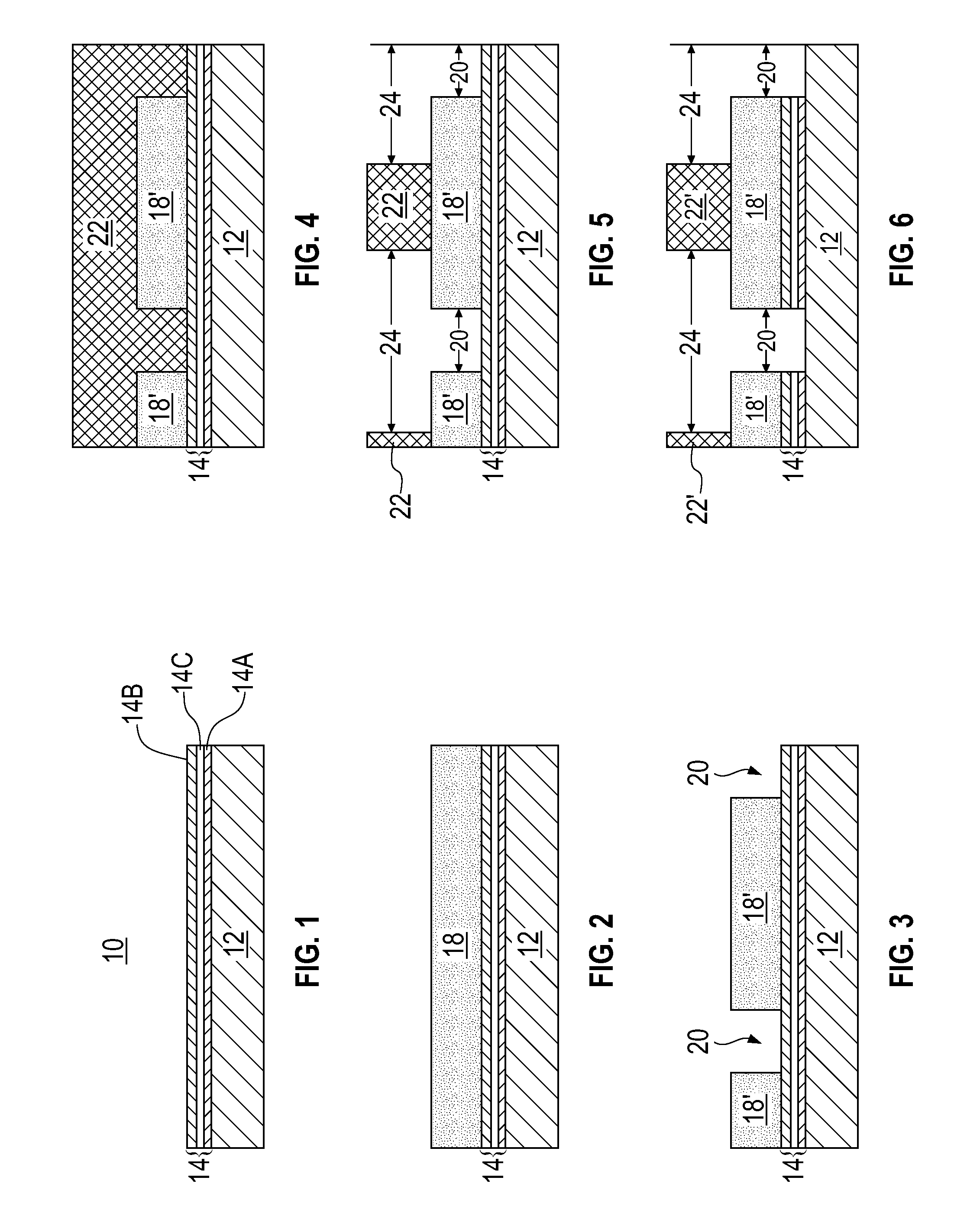
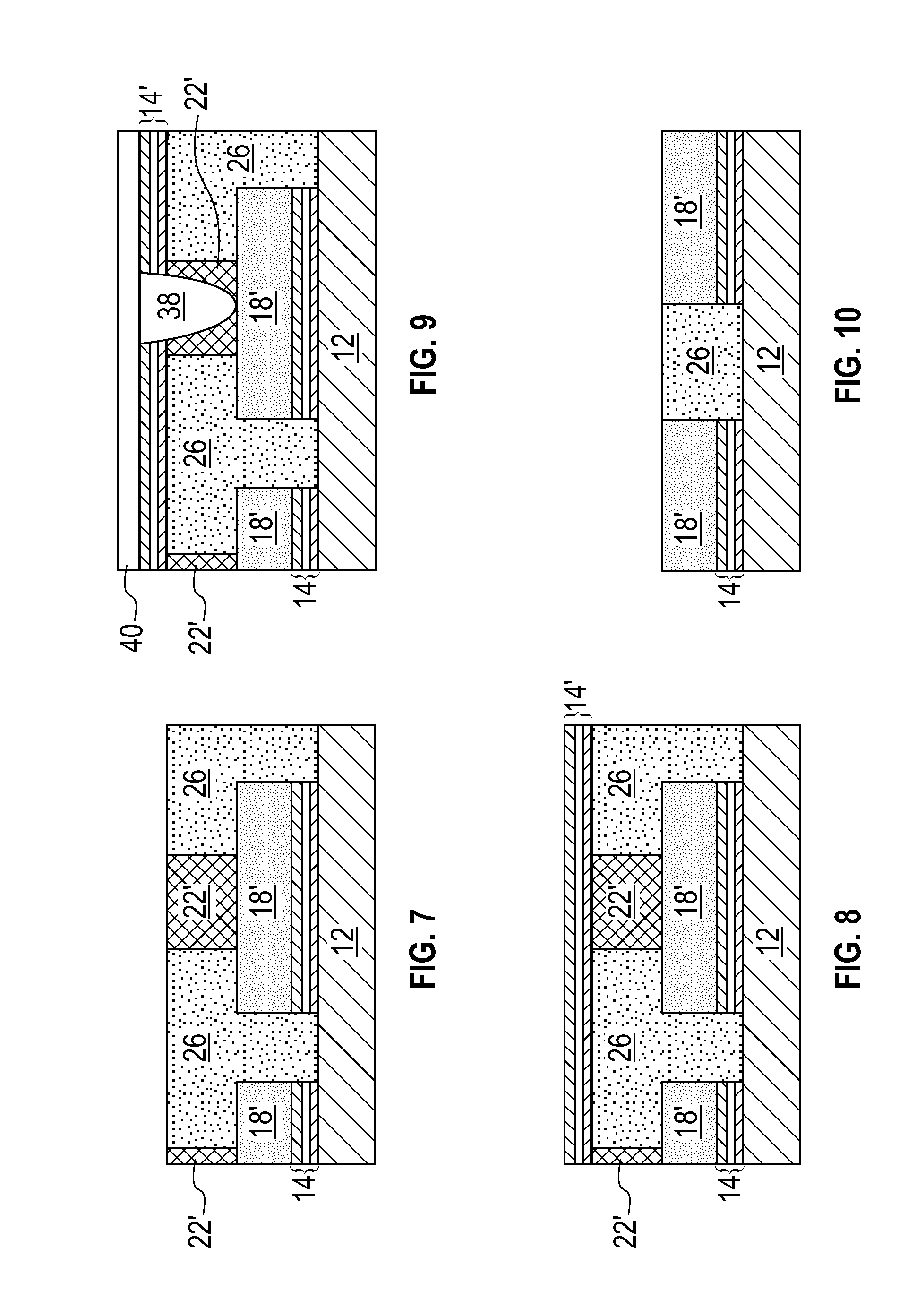
- Description
- Claims
- Application Information
AI Technical Summary
Benefits of technology
Problems solved by technology
Method used
Image

Examples
example 1
[0183]As summarized in the table below, five films were deposited onto silicon substrates at 400° C., high frequency rf power was varied between 300-460 Watts, and the pressure was varied between 3-8.7 torr. Trimethyl silane was selected as the carbon and silicon source, ammonia as the nitrogen source and He was used as a dilutant.
LayerTMS (sccm)NH3 (sccm)He (sccm)pressurepower180160200330021601602408.746031601003008.74604160503508.7460516004008.7460
[0184]The effect of varying trimethyl silane, ammonia flows was studied by FTIR (not shown). As shown in the FTIR spectra decreasing ammonia in the film decreases SiN and increases SiC, CH and SiH content in the film.
example 2
[0185]Using the individual conditions from layer 1-5 in example 1, a graded layer was deposited. Deposition time was varied for each layer to optimize film thickness and properties.
PUM
| Property | Measurement | Unit |
|---|---|---|
| Thickness | aaaaa | aaaaa |
| Thickness | aaaaa | aaaaa |
| Composition | aaaaa | aaaaa |
Abstract
Description
Claims
Application Information