Semiconductor device and method for manufacturing the same

a technology of semiconductor devices and semiconductors, applied in semiconductor devices, semiconductor/solid-state device details, electrical apparatus, etc., can solve problems such as chip dent, gap between the design value change in the distance between the circuit pattern and the lid, so as to reduce the dicing speed and the actual value, the effect of reducing the dicing accuracy and reducing the dicing speed

Active Publication Date: 2012-02-02
MITSUBISHI ELECTRIC CORP
View PDF1 Cites 17 Cited by
  • Summary
  • Abstract
  • Description
  • Claims
  • Application Information

AI Technical Summary

Benefits of technology

[0007]The body wafer and the lid wafer are joined in a vacuum by plasma activation joining or the like. At this time, the chip may dent due to difference between the atmospheric pressures of inside and outside of the device. In this case, distances to the circuit pattern and to the lid change, and problems of the gap between the designe

Problems solved by technology

At this time, the chip may dent due to difference between the atmospheric pressures of inside and outside of the device.
In this case, distances to the circuit pattern and to the lid change, and problems of the gap between the designed value and the actual value are caused.
Therefore,

Method used


Image

  • Semiconductor device and method for manufacturing the same
  • Semiconductor device and method for manufacturing the same
  • Semiconductor device and method for manufacturing the same

Examples


first embodiment

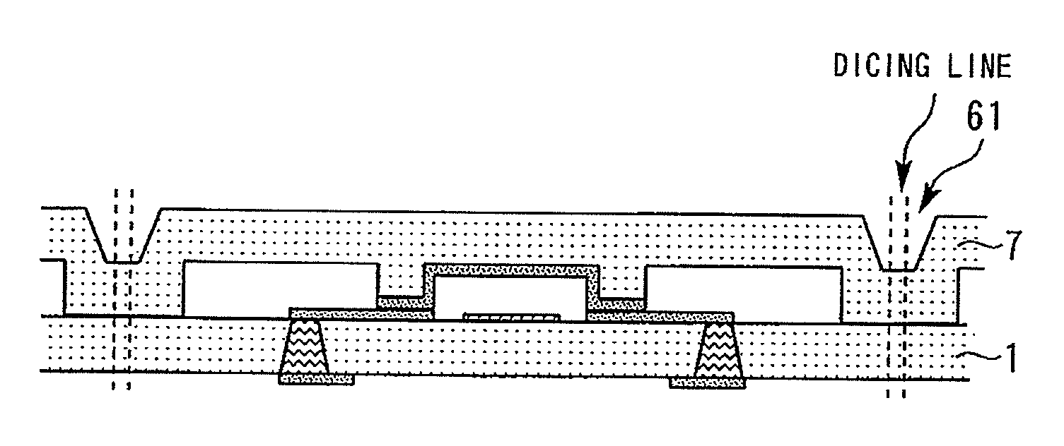
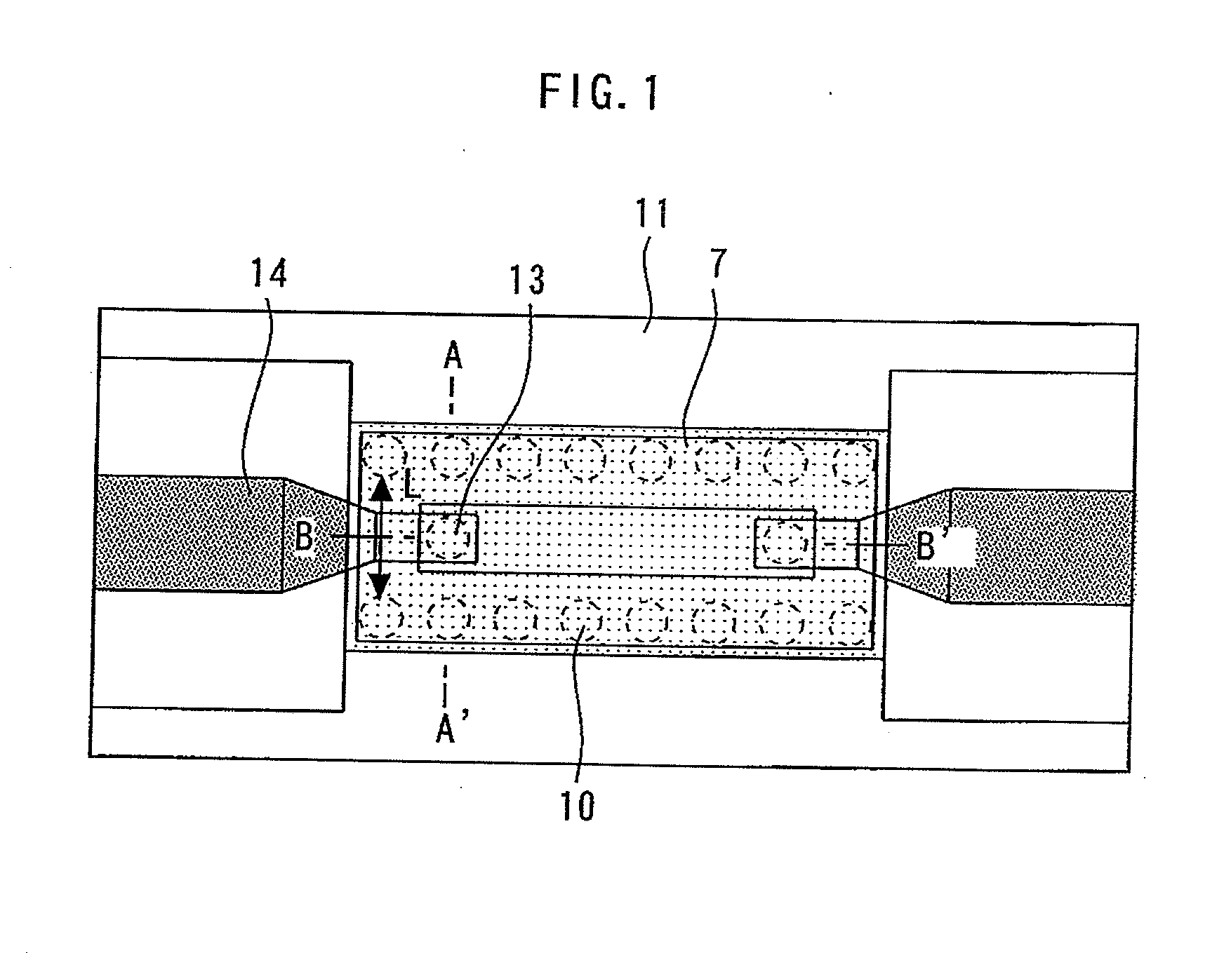
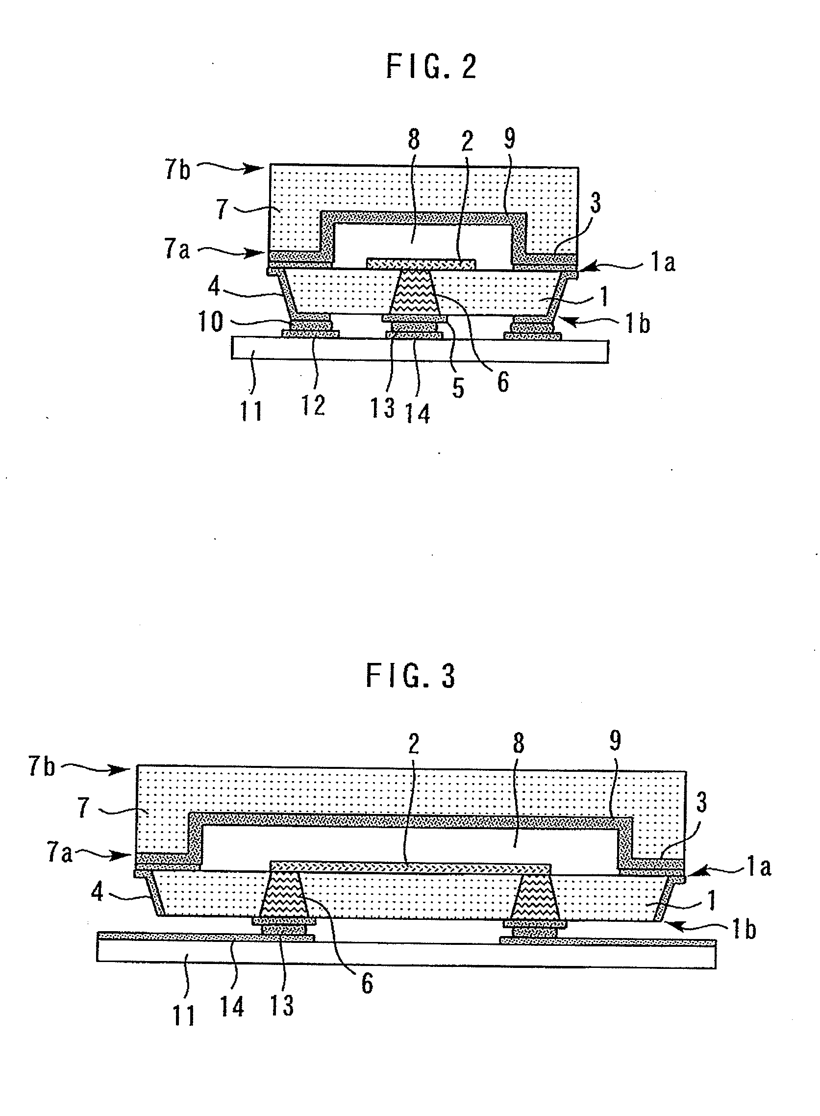
[0032]FIG. 1 is a plan view showing a semiconductor device according to the first embodiment. FIG. 2 is a sectional view taken along the line A-A′ in FIG. 1. FIG. 3 is a sectional view taken along the line B-B′ in FIG. 1.

[0033]A body wafer 1 has a major surface 1a and a major surface 1b facing to each other. A circuit pattern 2 and a metal film 3 are formed on the major surface 1a of the body wafer 1.

[0034]A metal film 4 is formed on the side surface of the body wafer 1 and a part of the major surface 1b, and the metal film 4 is connected to the metal film 3. A pad 5 for inputting / outputting signals is formed on the major surface 1b of the body wafer 1. The pad 5 for inputting / outputting signals is connected to the circuit pattern 2 by penetrating electrodes 6 penetrating through the body wafer 1.

[0035]The circuit pattern 2 is a circuit pattern for an amplifier and an oscillator, and has transistors, resistors, MIM capacitors, spiral inductors, wirings and the like. The through-hole...

second embodiment

[0052]A method for manufacturing a semiconductor device according to the second embodiment will be described. FIGS. 13 to 18 are sectional views for illustrating the method for manufacturing a semiconductor device according to the second embodiment.

[0053]First, in the same manner as in the first embodiment, steps shown in FIGS. 4 to 7 are performed. Next, as shown in FIG. 13, a metal film 19 and a recess 8 are formed on the major surface 7a of the lid wafer 7. Next, as shown in FIG. 14, a through-hole 20 penetrating the lid wafer 7 from the major surface 7b of the lid wafer 7 and reaching the metal film 19 is formed.

[0054]Next, as shown in FIG. 15, a metal film 21 is formed on the major surface 7b of the lid wafer 7, the inner wall of the through-hole 20, and the metal film 19 exposed in the through-hole 20.

[0055]Next, as shown in FIG. 16, a recess 8 is made to face to the circuit pattern 2, the through-hole 17 is aligned with the through-hole 20, and the metal film 3 is made to con...

third embodiment

[0059]A method for manufacturing a semiconductor device according to the third embodiment will be described. FIGS. 19 to 26 are sectional views for illustrating the method for manufacturing a semiconductor device according to the third embodiment.

[0060]First, as shown in FIG. 19, a circuit pattern 2 is formed on the major surface 1a of the body wafer 1.

[0061]Next, as shown in FIG. 20, a resist pattern 18 is formed on the major surface 7a of the lid wafer 7. The lid wafer 7 is subjected to etching using the resist pattern 18 as a mask. Thereby, a recess 8 is formed on the major surface 7a of the lid wafer 7.

[0062]Next, as shown in FIG. 21, the recess 8 is made to face to the circuit pattern 2, the semiconductors on the major surface 1a of the body wafer 1 are made to contact the semiconductors on the major surface 7a of the lid wafer 7, and the lid wafer 7 is joined to the body wafer 1 using plasma activation joining or the like.

[0063]Next, as shown in FIG. 22, the body wafer 1 and t...


PUM


Abstract

A method for manufacturing a semiconductor device comprises: forming a circuit pattern and a first metal film on a first major surface of a body wafer; forming a through-hole penetrating the body wafer from a second major surface of the body wafer and reaching the first metal film; forming a second metal film on a part of the second major surface of the body wafer, on an inner wall of the through-hole, and on the first metal film exposed in the through-hole; forming a recess on a first major surface of a lid wafer; forming a third metal film on the first major surface of the lid wafer including inside the recess of the lid wafer; with the recess facing the circuit pattern, and the first metal film contacting the third metal film, joining the lid wafer to the body wafer; and dicing the joined body wafer and lid wafer along the through-hole.

Description

BACKGROUND OF THE INVENTION[0001]1. Field of the Invention[0002]The present invention relates to a semiconductor device and a method for manufacturing the same wherein a lid wafer having a recess is joined to a body wafer having a circuit pattern.[0003]2. Background Art[0004]In recent years, applications using millimeter wave band, such as 60 GHz-band WPAN (Wireless Personal Area Network) and 76 GHz-band on-board millimeter wave radars, have been increased. These applications need semiconductor devices having high gain in millimeter wave band. Although a semiconductor device wherein semiconductor chips are sealed with a mold can reduce manufacturing costs, parasitic capacitance increases and the performance of the device deteriorates. In particular, the quantity of deterioration is marked in the millimeter wave band. In addition, the moisture resistance is not sufficiently maintained. Therefore, a semiconductor device wherein a lid wafer having a recess is joined to a body wafer hav...

Claims


Application Information

Patent Timeline
IPC IPC(8): H01L23/48H01L21/78
CPCH01L21/50H01L23/04H01L2924/00014H01L2924/1305H01L2924/1306H01L2924/01006H01L2924/01005H01L2924/16235H01L2924/10329H01L2924/01082H01L2924/01079H01L23/10H01L23/552H01L24/06H01L24/16H01L24/94H01L24/97H01L2224/0401H01L2224/0557H01L2224/06181H01L2224/16146H01L2224/16235H01L2224/94H01L2224/97H01L2924/01078H01L2224/81H01L2224/83H01L2924/00H01L2224/05552H01L2924/351
Inventor KANAYA, KOTSUKAHARA, YOSHIHIROWATANABE, SHINSUKE
Owner MITSUBISHI ELECTRIC CORP
Why Eureka
Try Eureka