Light-emitting element, light-emitting device, display device, and electronic apparatus

a technology of light-emitting devices and light-emitting elements, which is applied in the direction of thermoelectric devices, organic semiconductor devices, solid-state devices, etc., can solve the problems of phosphorescent materials, however, sensitive to impurities in the change of light-emitting properties, and the increase of driving voltage with the passage of time, so as to prevent the reduction of the electron transportability and electron injection properties of the re-type electron transport layer 51, the effect of enhancing

Inactive Publication Date: 2012-02-09
SEIKO EPSON CORP
View PDF6 Cites 13 Cited by
  • Summary
  • Abstract
  • Description
  • Claims
  • Application Information

AI Technical Summary

Benefits of technology

[0177]The sealing member 8 is provided so as to cover the anode 3, the layered structure 15, and the cathode 7 and has a function to seal each component to provide air proof, thereby blocking oxygen and moisture. The sealing member 8 is provided, thereby being able to provide advantageous effects, for example, in which the reliability of the light-emitting element 1 is improved and in which the quality of the light-emitting element 1 is prevented from being degraded and deteriorated (durability is enhanced).
[0178]Examples of a material of the sealing member 8 include Al, Au, Cr, Nb, Ta, Ti, or an alloy thereof; silicon oxide; and various resin materials. In the case where an electrically conductive material is used as the material of the sealing member 8, an insulating film is preferably provided between the sealing member 8 and the components including the anode 3, layered structure 15, and cathode 7 in order to prevent short circuit, where appropriate.
[0179]Furthermore, in order to obtain sealing, the sealing member 8 may be provided in the form of a plate so as to face the substrate 2, and a sealing material such as a thermosetting resin may be provided therebetween.
[0180]In the light-emitting element 1 having such a configuration, voltage is applied between the anode 3 and the cathode 7, thereby generating holes and electrons in the carrier-generating layer 5. The generated electrons are transported to the first light-emitting layer 42 and then recombine with holes injected from the anode 3, thereby contributing to light emission. On the other hands, the generated holes are transported to the second light-emitting layer 62 and the third light-emitting layer 63 and then recombine with electrons injected from the cathode 7, thereby contributing to light emission.
[0181]In the light-emitting element 1, accordingly, because the first light-emitting layer 42, second light-emitting layer 62, and third light-emitting layer 63 can each emit light, light emission efficiency can be enhanced, and a driving voltage can be reduced, as compared with a light-emitting element merely having a single light-emitting layer.
[0182]In particular, in the light-emitting element 1, the n-type electron transport layer 51 of the carrier-generating layer 5 contacts the first light-emitting layer 42, and the diffusion of the material contained in the n-type electron transport layer 51 (especially, electron donor material hereinafter described) to the layer on the side of the anode 3 (in this embodiment, the first light-emitting layer 42) can be therefore prevented or suppressed. Even in the case where the light-emitting element 1 is continuously driven at a constant current level for long time, the electron transportability and electron injection properties of the re-type electron transport layer 51 can be accordingly prevented from being decreased. The increase of the driving voltage of the light-emitting element 1 can be consequently suppressed.

Problems solved by technology

Unfortunately, traditional light-emitting elements have a problem in which the devices are continuously driven at a constant current level with the result that a driving voltage is significantly increased with the passage of time.
The phosphorescent material is, however, sensitive to impurities in the change of light-emitting properties.

Method used


Image

  • Light-emitting element, light-emitting device, display device, and electronic apparatus
  • Light-emitting element, light-emitting device, display device, and electronic apparatus
  • Light-emitting element, light-emitting device, display device, and electronic apparatus

Examples


example 1

First Process

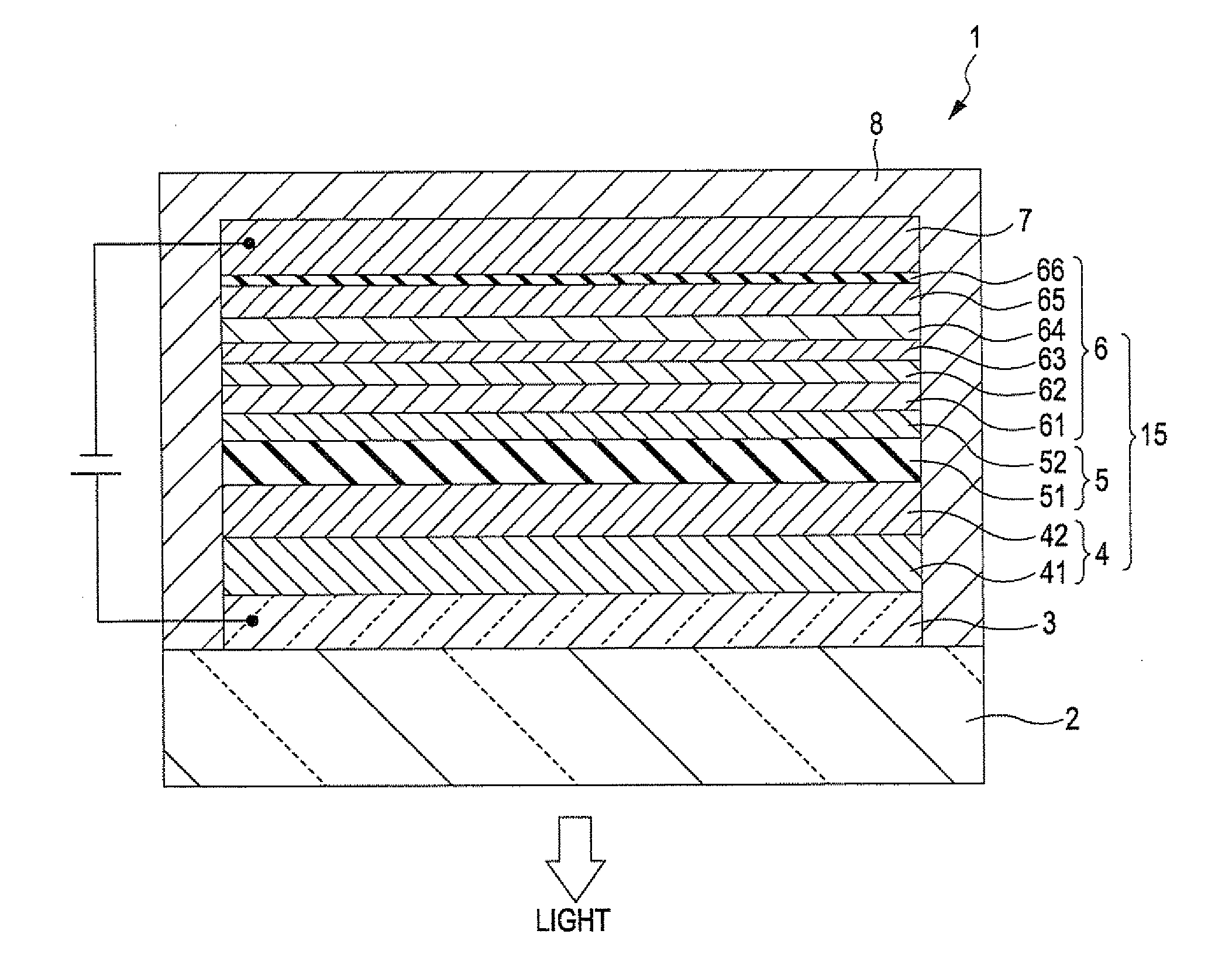
[0246]A transparent glass substrate having an average thickness of 0.5 mm was prepared. An ITO electrode (anode) was formed on the substrate by a spattering technique so as to have an average thickness of 50 nm.

[0247]The substrate was dipped in acetone and 2-propanol in sequence and was then subjected to ultrasonic cleaning.

[0248]The resultant product was then subjected to oxygen plasma treatment.

Second Process

[0249]Subsequently, N,N′-di(1-naphthyl)-N,N′-diphenyl-1,1′-biphenyl-4,4′-diamine (NPD) was deposited on the ITO electrode by a vacuum deposition method, thereby forming a hole transport layer (hole transport layer of a first light emitter) having an average thickness of 50 nm.

Third Process

[0250]A first light-emitting layer was subsequently formed on the hole transport layer by a vacuum deposition method so as to have an average thickness of 30 nm.

[0251]In this case, a mixed material of BD102 (commercially available from Idemitsu Kosan Co., Ltd.) as a blue light-em...

example 2

[0265]The process configurations the same as those in the example 1 were employed except that the first light-emitting layer was formed so as to have an average thickness of 45 nm and except that the n-type electron transport layer of the carrier-generating layer was formed so as to have an average thickness of 25 nm, thereby manufacturing a light-emitting element.

example 3

[0266]The process configurations the same as those in the example 1 were employed except that the first light-emitting layer was formed so as to have an average thickness of 65 nm and except that the n-type electron transport layer of the carrier-generating layer was formed so as to have an average thickness of 5 nm, thereby manufacturing a light-emitting element.


PUM


Abstract

A light-emitting element includes an anode; a cathode; a first light-emitting layer that is disposed between the anode and the cathode, the first light-emitting layer emitting light in response to application of voltage between the anode and the cathode; a second light-emitting layer that is disposed between the cathode and the first light-emitting layer, the second light-emitting layer emitting light in response to application of voltage between the anode and the cathode; and a carrier-generating layer that is disposed between the first light-emitting layer and the second light-emitting layer, the carrier-generating layer generating electrons and holes. The carrier-generating layer has an n-type electron transport layer and an electron-withdrawing layer, the n-type electron transport layer contacting the first light-emitting layer and having electron transportability, and the electron-withdrawing layer being disposed between the n-type electron transport layer and the second light-emitting layer and having electron-withdrawing properties.

Description

BACKGROUND[0001]1. Technical Field[0002]The present invention relates to a light-emitting element, light-emitting device, display device, and electronic apparatus.[0003]2. Related Art[0004]An organic electroluminescence device (namely, organic EL device) is a light-emitting element having a configuration in which at least one organic light-emitting layer is disposed between an anode and a cathode. In such a light-emitting element, an electric field is applied between the cathode and anode with the result that electrons are injected from the cathode to the light-emitting layer and that holes are injected from the anode to the light-emitting layer. The electrons then recombine with the holes in the light-emitting layer with the result that the excitons are generated. The excitons return to a ground state and thereby generate energy, and the energy is released in the form of light.[0005]One of a typical type of such a device has, for example, a configuration in which two or more light-...

Claims


Application Information

Patent Timeline
Patent Type & Authority Applications(United States)
IPC IPC(8): H01L51/52
CPCH01L27/3209H01L51/5016H01L2251/5346H01L51/5052H01L51/5278H01L51/5036H10K59/32H10K50/125H10K50/11H10K2101/10H10K50/165H10K50/19H10K2101/80
Inventor MITSUYA, MASAYUKI
Owner SEIKO EPSON CORP
Why Eureka
Try Eureka