Substrate Structure of LED (light emitting diode) Packaging and Method of the same

a technology of light-emitting diodes and substrate structures, which is applied in the direction of semiconductor/solid-state device manufacturing, electrical equipment, semiconductors, etc., can solve the problems of shortening the life of led, changing the wavelength of light emitted, and the conventional package existing to date is inadequate for the demands of many current and future led applications, so as to achieve the effect of enhancing light-emitting efficiency and conducting heat more efficiently

Inactive Publication Date: 2012-02-16
KING DRAGON INT
View PDF3 Cites 72 Cited by
  • Summary
  • Abstract
  • Description
  • Claims
  • Application Information

AI Technical Summary

Benefits of technology

[0009]The present invention provides a substrate structure for a LED packaging to overcome the aforementioned problems in the prior art. The substrate has the structure with plurality of Copper (Cu) filled via holes to conduct heat more efficiently and with the cavity metal as a reflector to enhance the light emitting efficiency.

Problems solved by technology

Given that the heat cannot dissipate immediately, the junction temperature of the semiconductor device will increase; and the higher junction temperature is, the lower of light emitting efficiency and the shorter of lifetime of LED will be.
Besides, the increased temperature will also change the wavelength of light emitted by LED, which is not wanted in applications.
Most conventional packages existing to date are inadequate for the demands of many current and future LED applications.
Most current LED packages use ceramic substrate, such as Al2O3, AlN, and those need heat sink to dissipate the power efficiently due to the poor thermal conductivity of ceramics.

Method used


Image

  • Substrate Structure of LED (light emitting diode) Packaging and Method of the same
  • Substrate Structure of LED (light emitting diode) Packaging and Method of the same
  • Substrate Structure of LED (light emitting diode) Packaging and Method of the same

Examples


Embodiment Construction

[0036]Structure and method for manufacturing a substrate for an Optical device is described below. In the following description, more detail descriptions are set forth in order to provide a thorough understanding of the present invention and the scope of the present invention is expressly not limited expect as specified in the accompanying claims.

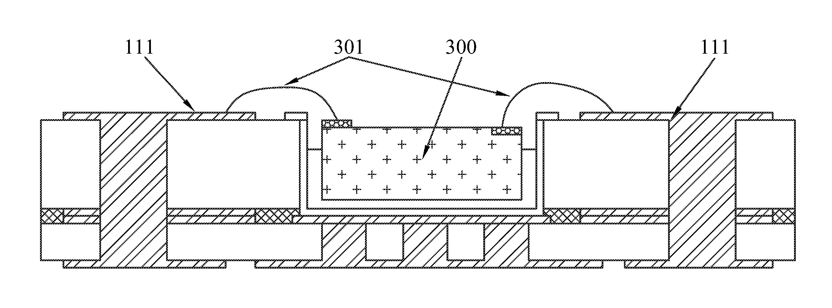
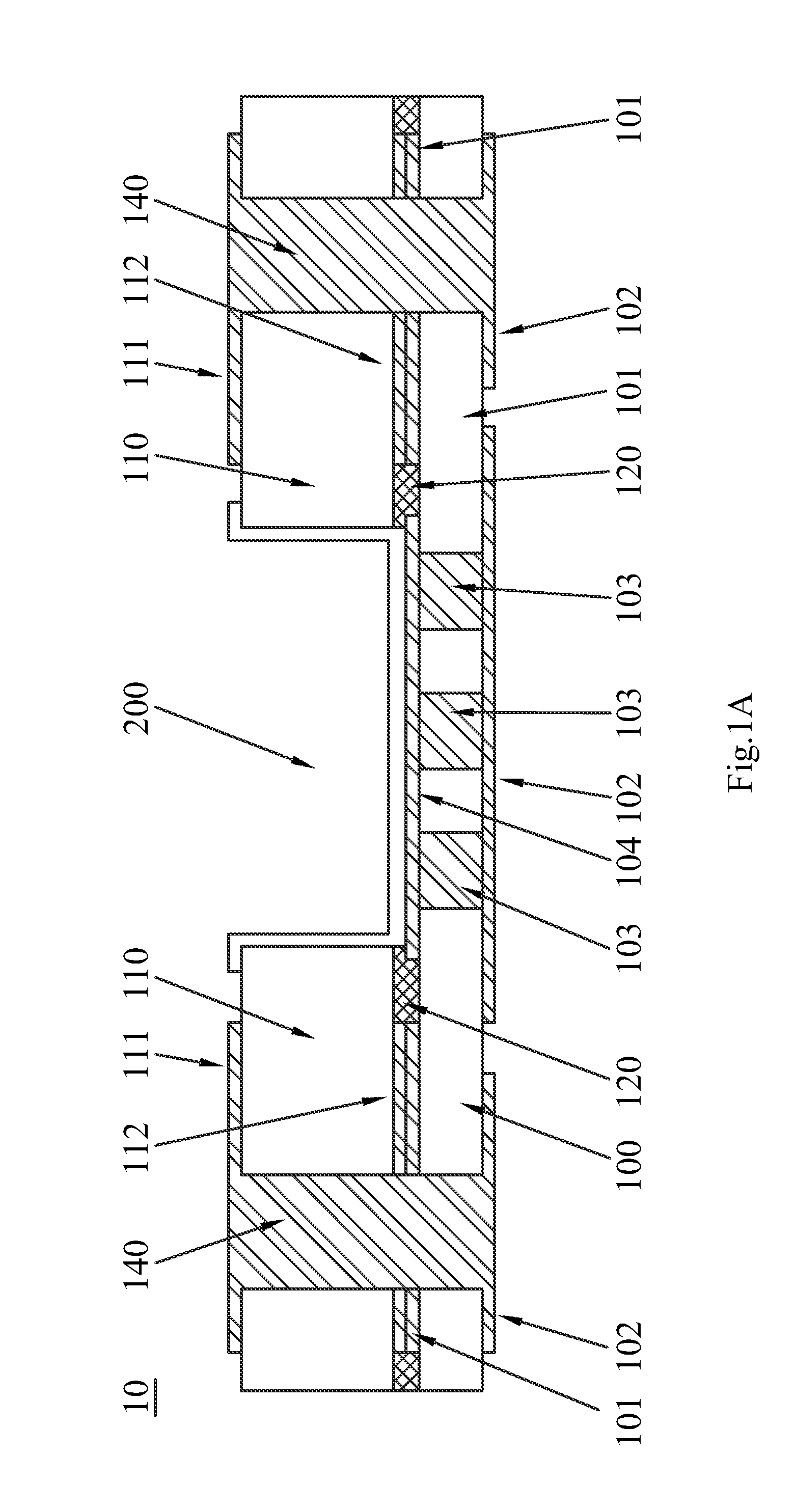
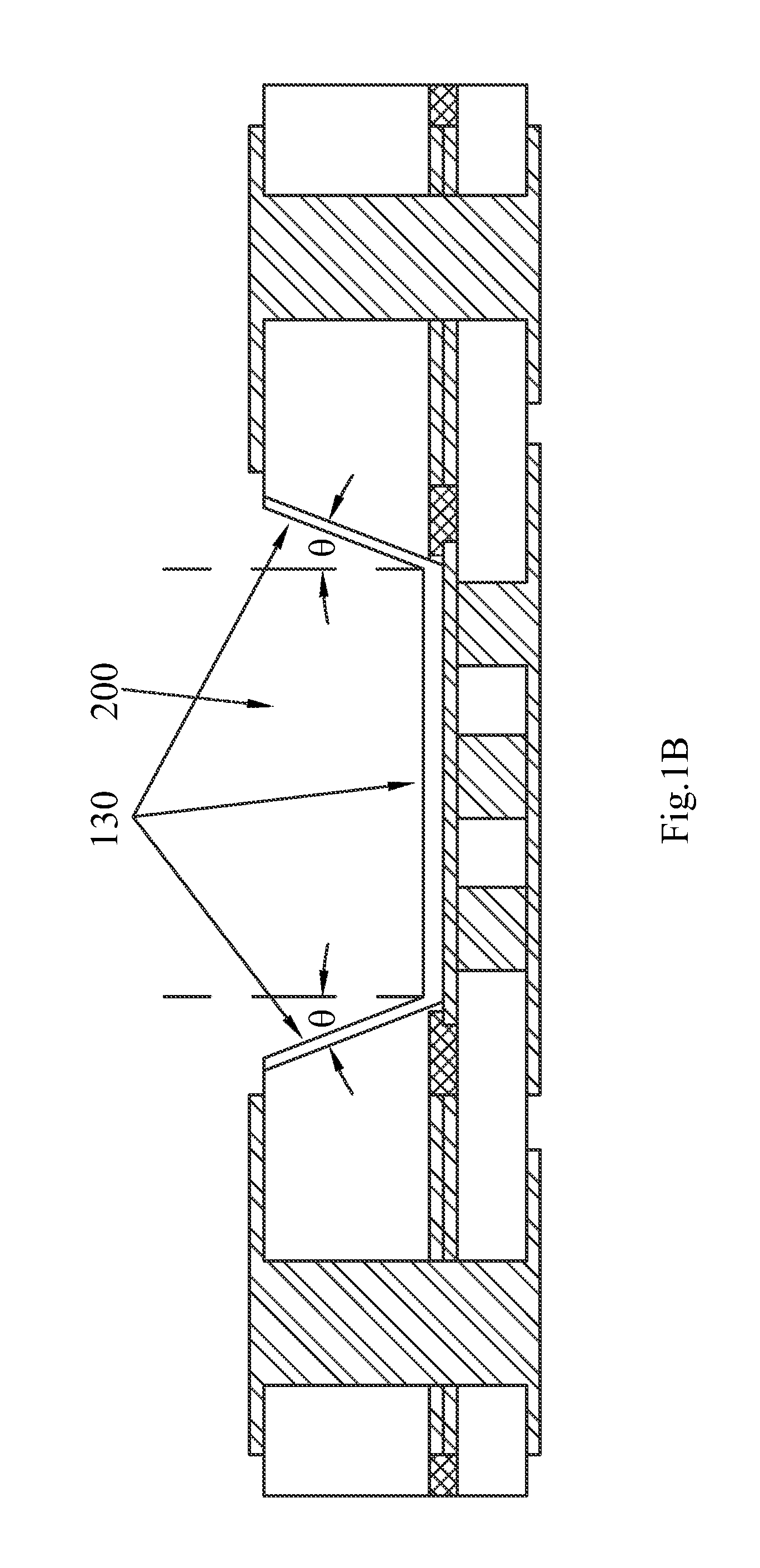
[0037]A substrate structure 10 with a cavity for carrying an optical device, such as LED (lighting emitting diode), Laser Diode, Photo Diode, Photo detector etc, is disclosed. As shown in FIG. 1A, the substrate structure 10 includes a first substrate 100 and a second substrate 110. The first substrate 100 has a die metal pad 104 for carrying an LED, a first wiring circuit 101 is on the top surface of the first substrate 100, while a second wiring circuit 102 is on the bottom surface of the first substrate 100, and a plurality of via holes 103 are filled with metal, alloy such as Cu or the like.

[0038]The second substrate110 has a die opening...


PUM

PropertyMeasurementUnit
thicknessaaaaaaaaaa
temperatureaaaaaaaaaa
thicknessaaaaaaaaaa

Abstract

The present invention provides a substrate for LED packaging and a fabrication method thereof. The substrate can dissipate heat quickly and enhance light emitting efficiency. For this purpose, several via holes are formed in the substrate and metal layers are coated to act as light reflector. In the substrate, the via holes are filled with the material with high thermal conductivity, such as Copper, to conduct the heat efficiently; and the reflector are coated the metal with high reflection factor to visible light, such as Ag, Au, Al, to enhance the light emitting efficiency.

Description

BACKGROUND[0001]1. Technical Field[0002]This invention relates to a substrate structure for an LED packaging, and more particularly to a substrate structure which can dissipate heat efficiently, and thus improve the light conversion efficiency and the lifespan of the LED.[0003]2. Description of the Related Art[0004]LED is more and more used in many applications, such as lighting, display, indicator etc. LED is a semiconductor device wherein electrical energy is directly converted into optical energy, within a very narrow wavelength range. The light output of an LED is proportional to the forward current which is the function of forward voltage applied.[0005]While in operation, only about 20% of electrical energy applied to LED is converted to visual light and the rest of energy, about 80%, is converted to heat. Given that the heat cannot dissipate immediately, the junction temperature of the semiconductor device will increase; and the higher junction temperature is, the lower of lig...

Claims


Application Information

Patent Timeline
Patent Type & Authority Applications(United States)
IPC IPC(8): H01L33/48H01L33/00
CPCH01L31/0203H01L33/486H01L33/60H01L33/62H01L33/641H01L33/642H01L2933/0033H01L2224/32225H01L2224/48227H01L2224/73265H01L2224/48091H01L2924/00014H01L2924/00H01L2924/00012H01L24/73
Inventor YANG, WEN-KUN
Owner KING DRAGON INT
Why Eureka
Try Eureka