
Thermal enhancement for multi-layer semiconductor stacks

a multi-layer semiconductor and stack technology, applied in the direction of individual semiconductor device testing, semiconductor/solid-state device testing/measurement, instruments, etc., can solve the problems of increasing the cost of manufactured chips, reducing the yield of the manufacturing process, and data between the various functional units of the semiconductor chip can become a bottleneck on overall performance, etc., to achieve the effect of increasing the thermal conductivity of the multi-layer semiconductor stack and increasing the thermal conductivity

Active Publication Date: 2012-02-16
GLOBALFOUNDRIES US INC
View PDF2 Cites 58 Cited by
  • Summary
  • Abstract
  • Description
  • Claims
  • Application Information

AI Technical Summary

Benefits of technology

[0011]The invention also addresses the aforementioned problems by providing a circuit arrangement and method that in another aspect organize the circuit layers in a multi-layer semiconductor stack based upon current density so as to reduce power distribution losses in the stack. In particular, embodiments consistent with the invention recognize that through improved thermal characteristics of semiconductor dies used in a multi-layer semiconductor stack relative to a conventional single layer semiconductor die, the arrangement of circuit layers may be selected to optimize power distribution losses and thereby minimize IR drops and effective DC resistance in a stack.
[0012]Therefore, consistent with another aspect of the invention, a circuit arrangement includes a plurality of semiconductor dies physically and electrically coupled to one another in a stack, with each semiconductor die including opposing faces, where at least one face of each semiconductor die includes circuit logic integrated thereon and defining a circuit layer that includes at least one functional unit, where at least one face of each semiconductor die includes an inter-layer interface region disposed thereon, and where each inter-layer interface region on each semiconductor die is disposed at substantially the same topographic location when the respective semiconductor die is disposed within the stack. The circuit arrangement also includes an inter-layer bus electrically coupling the functional units on the plurality of semiconductor dies to one another, with the inter-layer bus comprising a plurality of electrical conductors disposed within the inter-layer interface region of each semiconductor die and extending between the opposing faces of each semiconductor die, where respective electrical conductors disposed in the inter-layer interface regions of adjacent semiconductor dies in the stack are electrically coupled to one another when the plurality of circuit layers are physically and electrically coupled to one another in the stack, where the stack includes bottom and top opposing faces respectively defined on bottom and top semiconductor dies from among the plurality of semiconductor dies, where the bottom face is configured to mount the stack to a substrate, and where the top face is configured to interface with a heat sink, and where the plurality of semiconductor dies are arranged in the stack such that a first semiconductor die having a higher current density than a second semiconductor die is disposed closer to the bottom face of the stack than the second semiconductor die to reduce power distribution losses in the stack.

Problems solved by technology

In addition, as feature sizes decrease, and thus as faster and more complex circuits are integrated onto a given semiconductor chip, architects are finding that in many instances the communication of data between the various functional units on a semiconductor chip can become a bottleneck on overall performance.
Furthermore, in general as the size and amount of circuitry integrated into a chip design increases, the yield of the manufacturing process typically decreases, thereby increasing the cost of the manufactured chips.
From a design standpoint, however, integrating circuits on multiple chips in a multi-layer semiconductor stack can be problematic.
Laying out signal paths and electrical conductors to effectively interconnect circuits conventionally has required substantial design work, and opportunities for design reuse have been limited.
Another challenge for multi-layer semiconductor stacks is thermal dissipation.
However, with multi-layer semiconductor stacks, the same amount of logic circuitry, and thus the same amount of heat generating circuitry, can present a much smaller surface area to which a heat sink may be mounted.

Method used


Image

  • Thermal enhancement for multi-layer semiconductor stacks
  • Thermal enhancement for multi-layer semiconductor stacks
  • Thermal enhancement for multi-layer semiconductor stacks

Examples


Embodiment Construction

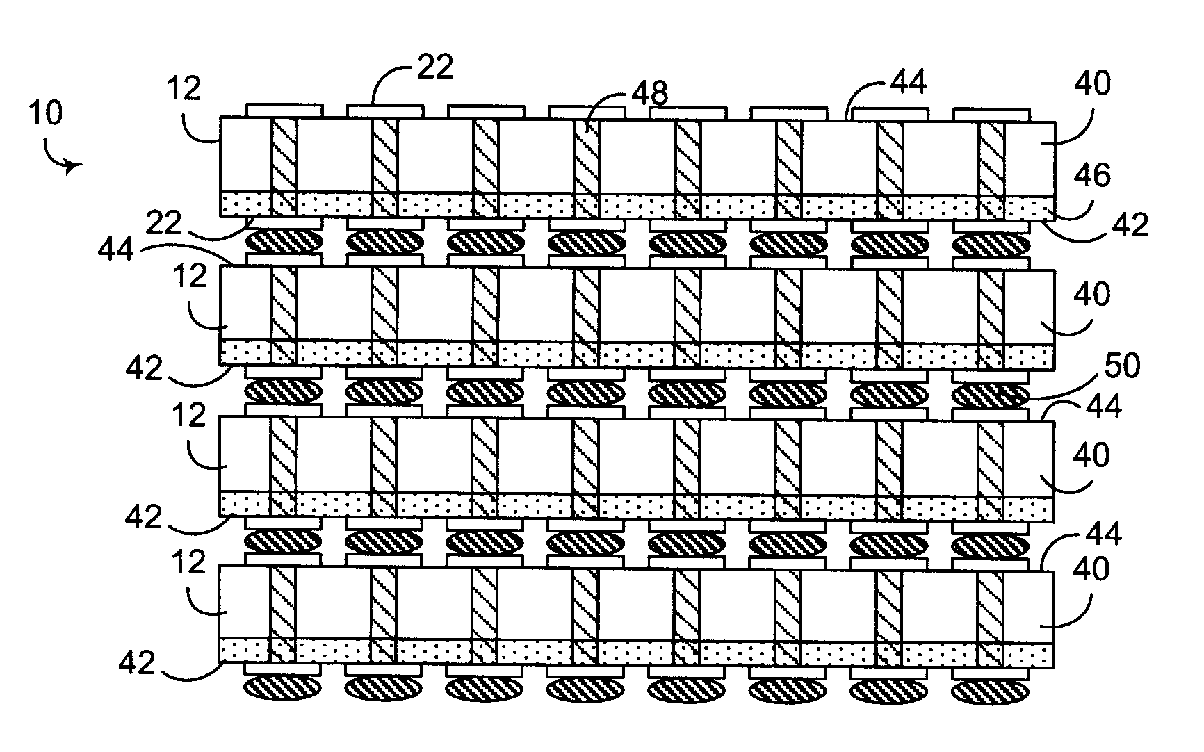
[0034]Embodiments consistent with the invention may incorporate techniques consistent with the invention to enhance the thermal characteristics of a multi-layer semiconductor stack. One technique that may be employed utilizes thermal-only through vias (hereinafter referred to as “thermal vias”) to improve the thermal conductivity of a multi-layer semiconductor stack. Another technique, which may be used in connection with or in lieu of thermal vias, sequences or arranges semiconductor dies, and the circuit layers disposed thereon, in a stack so as to minimize power distribution losses in the stack.

[0035]Prior to discussing the aforementioned thermal enhancement techniques, however, an overview of one implementation of a multi-layer semiconductor stack and the design thereof, suitable for use in connection with such thermal enhancement techniques, is provided.

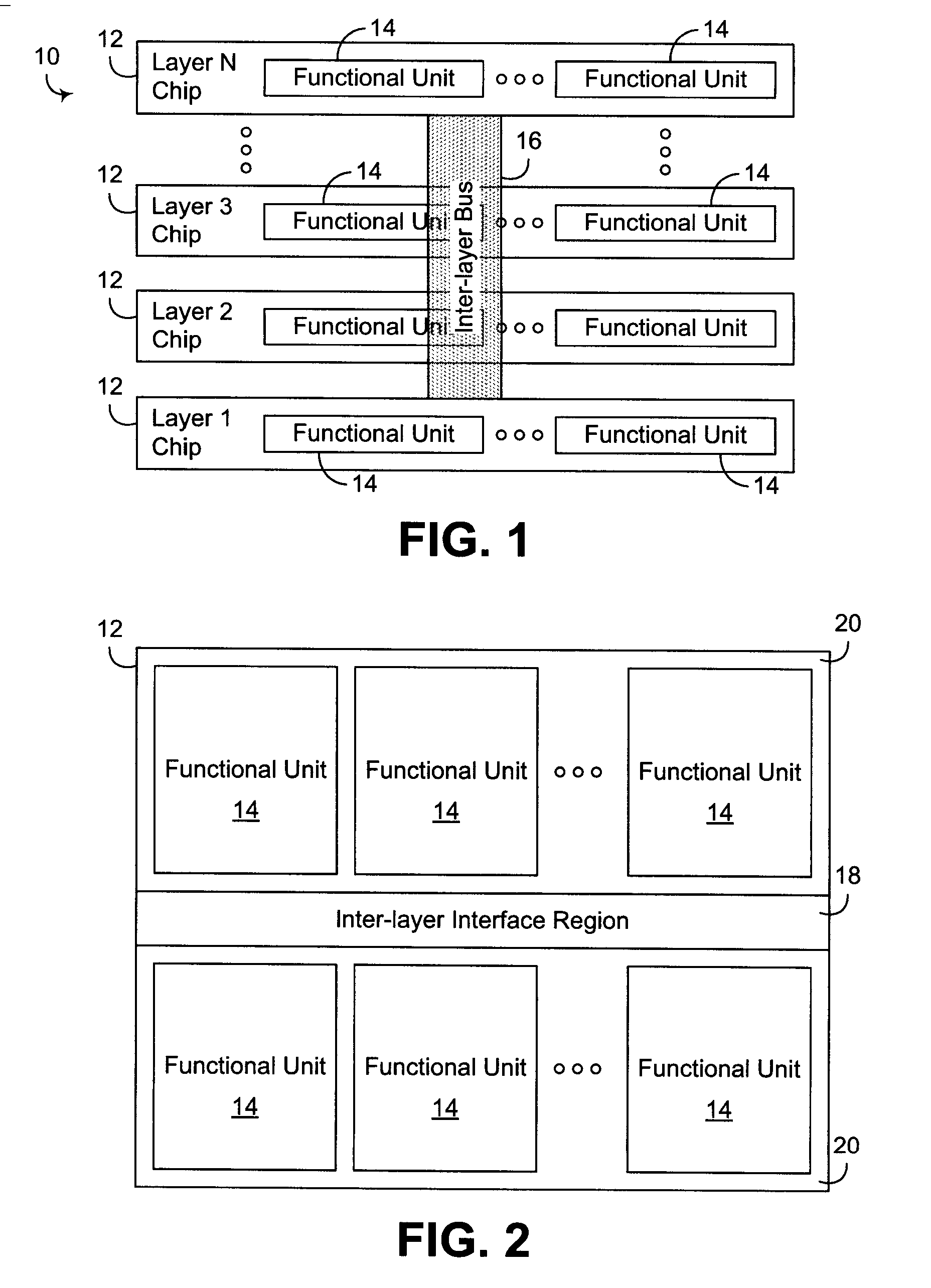
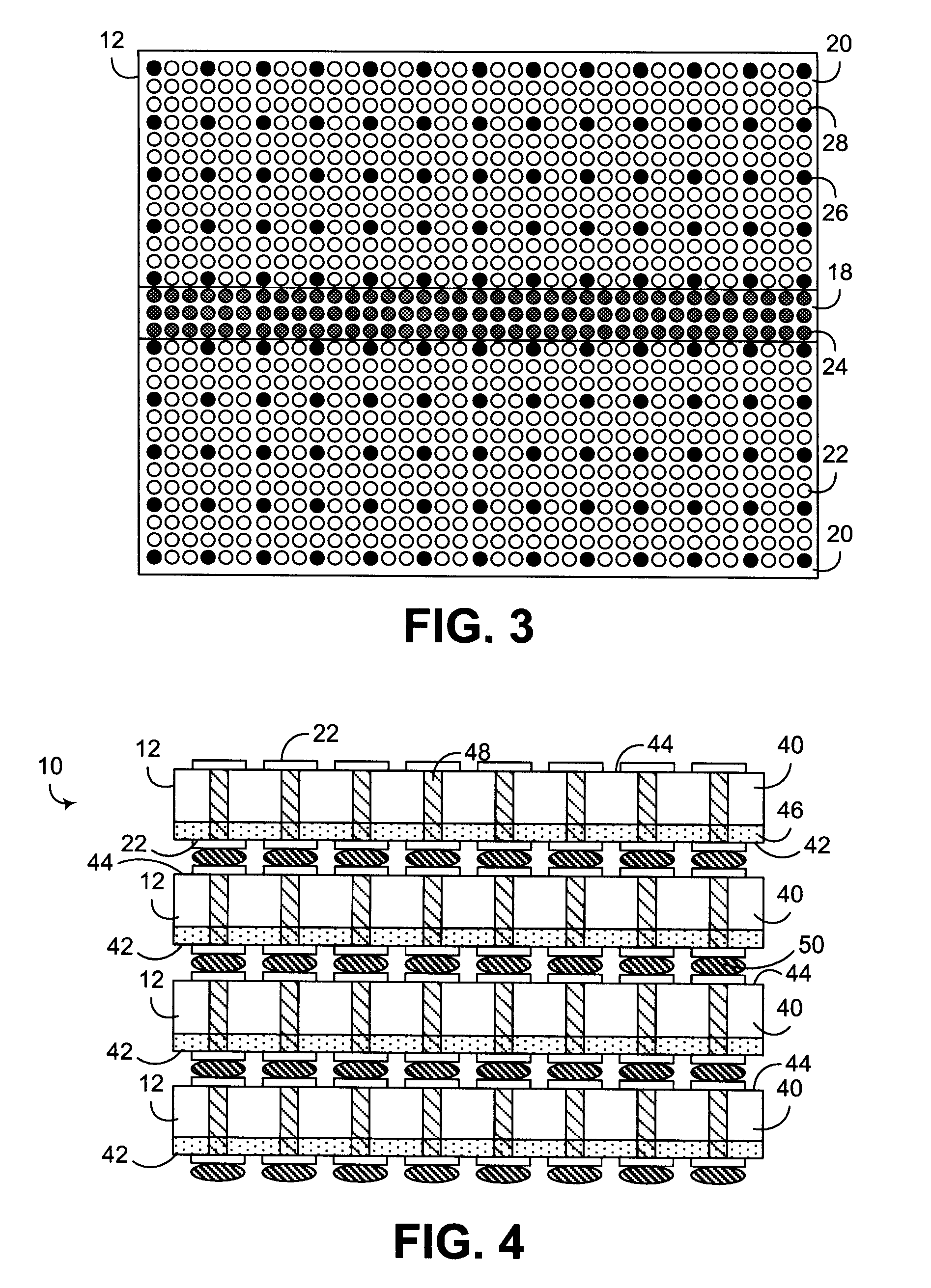
[0036]Multi-Layer Semiconductor Stack with Inter-Layer Bus

[0037]Embodiments of the invention may be utilized in connection wit...


PUM


Abstract

A circuit arrangement and method in one aspect utilize thermal-only through vias, extending between the opposing faces of stacked semiconductor dies, to increase the thermal conductivity of a multi-layer semiconductor stack. The thermal vias are provided in addition to data-carrying through vias, which communicate data signals between circuit layers, and power-carrying through vias, which are coupled to a power distribution network for the circuit layers, such that the thermal conductivity is increased above that which may be provided by the data-carrying and power-carrying through vias in the stack. A circuit arrangement and method in another aspect organize the circuit layers in a multi-layer semiconductor stack based upon current density so as to reduce power distribution losses in the stack.

Description

CROSS-REFERENCE TO RELATED APPLICATIONS[0001]This application is related to U.S. patent application Ser. No. 12 / 431,259 filed on Apr. 28, 2009 by Bartley et al., which application is incorporated by reference herein.FIELD OF THE INVENTION[0002]The invention is generally related to interconnecting multiple semiconductor dies in a stack and the design of circuit logic therefor.BACKGROUND OF THE INVENTION[0003]As semiconductor technology continues to inch closer to practical limitations in terms of feature size, architects are increasingly focusing on alternative manners of meeting the demands for integrating increasingly complex circuitry onto semiconductor devices, or chips. In addition, as feature sizes decrease, and thus as faster and more complex circuits are integrated onto a given semiconductor chip, architects are finding that in many instances the communication of data between the various functional units on a semiconductor chip can become a bottleneck on overall performance. ...

Claims


Application Information

Patent Timeline
IPC IPC(8): H01L23/538G06F17/50H01L21/50
CPCG06F17/5068H01L23/3677H01L23/481H01L23/49838H01L23/50H01L24/05H01L24/06H01L24/16H01L25/0657H01L2224/0401H01L2224/0557H01L2224/0612H01L2224/06181H01L2224/06519H01L2224/16145H01L2224/16146H01L2225/06513H01L2225/06541H01L2225/06565H01L2225/06589H01L2924/01013H01L2924/01082H01L2924/014H01L2924/01033H01L2924/01077H01L2924/14H01L2924/00H01L2924/00014H01L2224/05552G06F30/39
Inventor BARTLEY, GERALD K.HOOVER, RUSSELL D.JOHNSON, CHARLES L.VANDERWIEL, STEVEN P.
Owner GLOBALFOUNDRIES US INC
Learn More