CMOS sensor with low partition noise and low disturbance between adjacent row control signals in a pixel array

a pixel array and control signal technology, applied in the field of cmos image sensor row control circuit, can solve the problems of noise, degrade the performance of the image sensor, and several transfer transistors,

Active Publication Date: 2012-02-23
TAIWAN SEMICON MFG CO LTD
View PDF6 Cites 23 Cited by
  • Summary
  • Abstract
  • Description
  • Claims
  • Application Information

AI Technical Summary

Benefits of technology

[0013]Bae et al. describe various slew rate control implementations for buffer 12 that can improve the partition noise of the CMOS image sensor. Specifically, these embodiments increase the falling time of the transfer control signal applied to the gate of the transfer transistor. In a first embodiment, shown in FIG. 4, the falling time of the control signal is increased by reducing a W / L ratio of an NMOS transistor N1 of the CMOS inverter of buffer 12. Specifically, a resistance through the transistor N1 can be increased, i.e., a current is decreased, by increasing the length L or decreasing the width W, thereby increasing the falling time of the transfer control signal. Meanwhile, the width W of the gate electrode is related to the design rule of the device. Accordingly, a method of reducing the W / L ratio without modifying the design rule is to increase the length L of the gate electrode when the width W of the NMOS transistor is fixed.

Problems solved by technology

Meanwhile, the transfer transistor TX has several problems when a transfer control signal applied to a gate of a transfer transistor is dropped from a logic level ‘HIGH’ to a logic level ‘LOW’, that is, when it changes from a turned-on state to a turned-off state.
Therefore, when seen from the outside, it appears that noise occurs.
Since the partition noise is considered as noise on a screen, it acts as a factor that degrades the performance of the image sensor.
As can be seen from slope lines 22, there is a wide distribution in the slopes of the down transition of the control signal TX[0] to TX[n], which results in different charge injection at individual pixels and clock-feed through, which manifests as partition noise.
Specifically, these embodiments increase the falling time of the transfer control signal applied to the gate of the transfer transistor.
Another important problem that arises in the use of CMOS image sensors is the coupling of control signals between adjacent rows due to parasitic coupling capacitances between adjacent rows (labeled Cc in FIG. 2).
The prior art discussed above addresses the partition noise problem but does not address coupling noise and other issues attributable to these parasitic capacitances.
In fact, the slew rate control approaches of the prior art can exacerbate the problems associated with coupling of adjacent signals between rows.
However, due to the high NMOS resistances in the drivers, the control signals for pulling the unselected row are weak and adjacent signals from an active row are easily coupled to the inactive row.
This results in low power efficiency due to leakage current or even improper operation of the CMOS image sensor.

Method used


Image

  • CMOS sensor with low partition noise and low disturbance between adjacent row control signals in a pixel array
  • CMOS sensor with low partition noise and low disturbance between adjacent row control signals in a pixel array
  • CMOS sensor with low partition noise and low disturbance between adjacent row control signals in a pixel array

Examples


Embodiment Construction

[0037]This description of the exemplary embodiments is intended to be read in connection with the accompanying drawings, which are to be considered part of the entire written description. Terms concerning electrical attachments, coupling and the like, such as “connected” and “interconnected,” refer to a relationship wherein structures communicate with one another either directly or indirectly through intervening structures, unless expressly described otherwise.

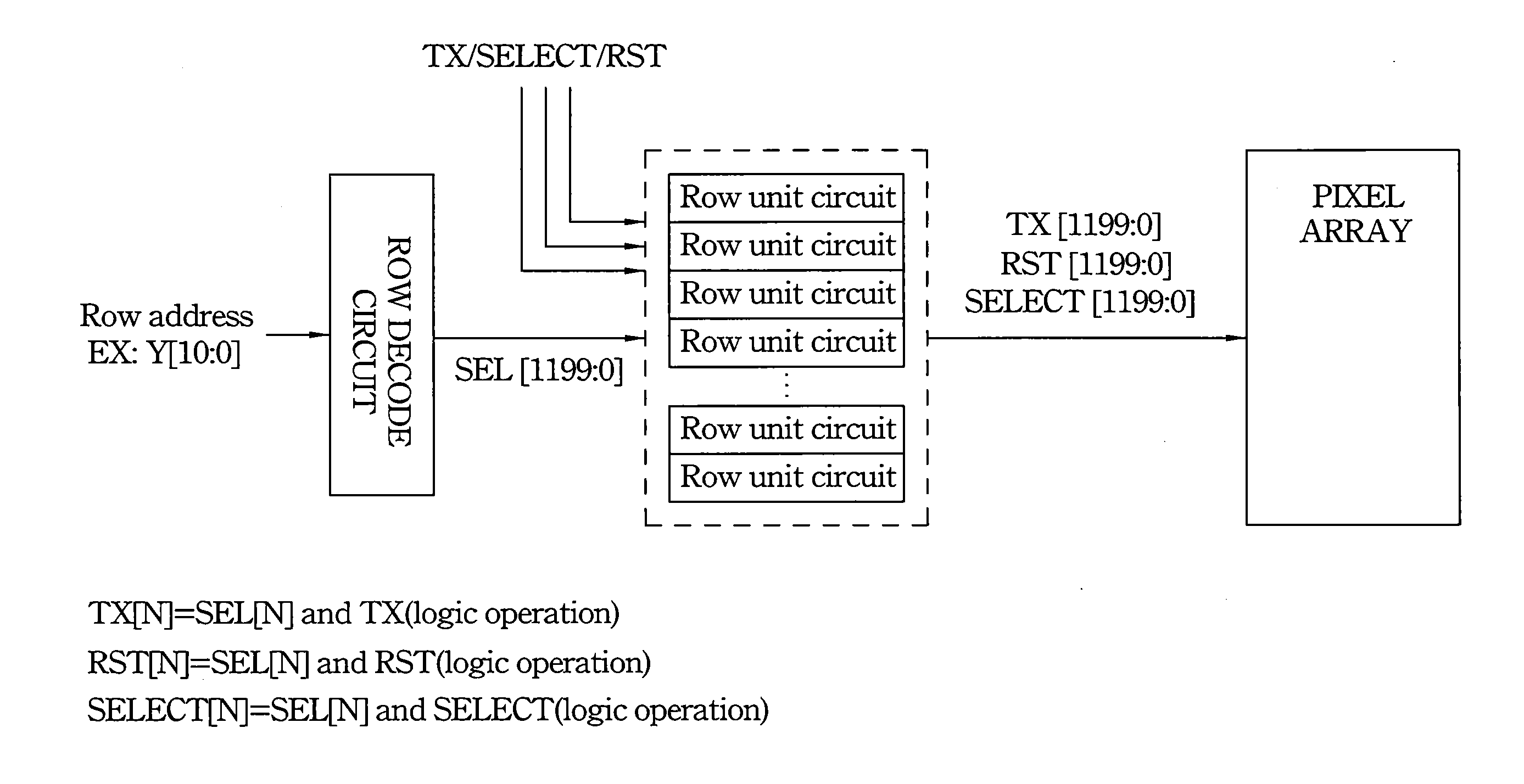
[0038]An improved image sensor, such as a CMOS image sensor, is described below in connection with the drawings. In embodiments of the sensor, the CMOS image sensor is configured to reduce both partition noise of the CMOS image sensor and the disturbance between adjacent row control signals.

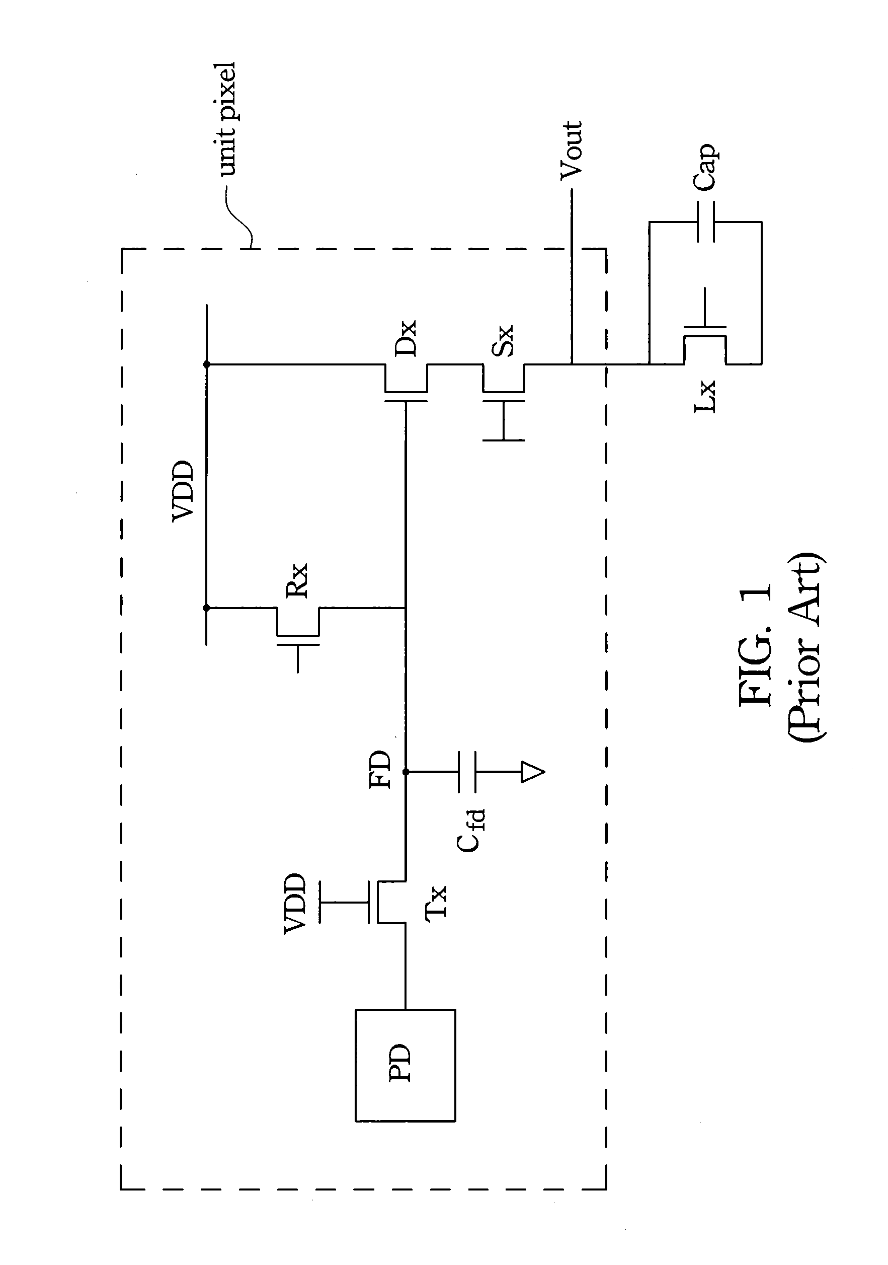
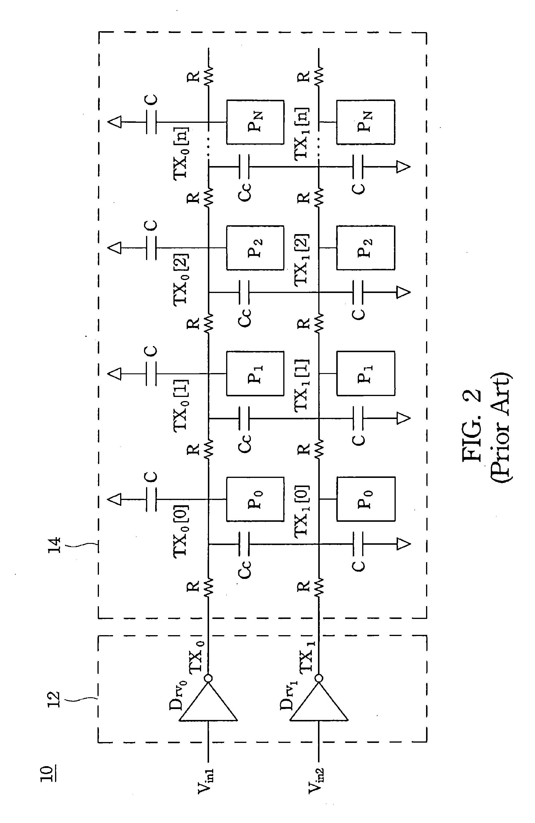
[0039]FIG. 6 is a circuit diagram of an embodiment of the present invention of a CMOS image sensor 100 having a buffer 62 for providing row control signals and a pixel array 64 with two adjacent row control signal lines, X and Y. While only...


PUM


Abstract

A CMOS image sensor includes a pixel array including a plurality of unit pixels with individual rows of unit pixels being coupled to respective row control signal lines, and a buffer including plural row control signal drivers. Each driver is coupled to a respective one of the row control signal lines and is configured to provide a row control signal pulse to a respective row control signal line in response to an input pulse when the row control signal line is in an active state and to bias the row control signal line at a ground voltage when the respective row control signal line is in an inactive state. Each driver has a first drive capability when the row control signal line is in the active state and a second drive capability greater than the first drive capability when the row control signal line is in an inactive state.

Description

FIELD OF THE INVENTION[0001]The present invention relates to a row control circuit of a CMOS image sensor, and more particularly to schemes for reducing partition noise and disturbance between adjacent row control signals.BACKGROUND OF THE INVENTION[0002]An image sensor is a semiconductor device that converts an optical image into an electric signal. One such image sensor is the complementary metal oxide semiconductor (hereinafter, referring to a CMOS) image sensor. The CMOS image sensor includes a plurality of unit pixels fabricated through CMOS processes. Each of the unit pixels includes one photodiode and three or four MOS transistors for driving the unit pixel. The CMOS image sensor employs CMOS technology that uses a control circuit and a signal processing circuit as a peripheral circuit. The MOS transistors are formed based on the number of pixels, while the output data is successively detected through the use of the MOS transistors.[0003]In fabricating these various kinds of ...

Claims


Application Information

Patent Timeline
Patent Type & Authority Applications(United States)
IPC IPC(8): H04N5/335
CPCH04N5/3577H01L27/14643H04N5/376H04N5/374H04N25/617H04N25/74H04N25/76
Inventor CHOU, KUO-YUCHAO, CALVIN YI-PING
Owner TAIWAN SEMICON MFG CO LTD
Why Eureka
Try Eureka