Diffusion Sources From Silicon Based Liquid Precursors

Active Publication Date: 2012-03-01
CHEMTRON RES
View PDF2 Cites 16 Cited by
  • Summary
  • Abstract
  • Description
  • Claims
  • Application Information

AI Technical Summary

Problems solved by technology

The practical requirements of the heavy phosphorous doping in the emitter region suffer from drawbacks, for example, high surface recombina

Method used


Image

  • Diffusion Sources From Silicon Based Liquid Precursors
  • Diffusion Sources From Silicon Based Liquid Precursors
  • Diffusion Sources From Silicon Based Liquid Precursors

Examples


example 1

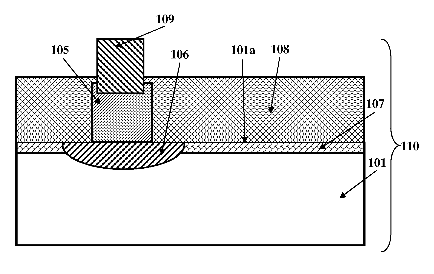
[0047]A doped liquid precursor is locally deposited on the substrate wafer 101 to create a local area doped polysilane film 102 on the surface 101a. The substrate wafer 101 with the doped polysilane film 102 is heated to diffuse the dopants into the substrate wafer 101 to create a heavily diffused region 106 in the substrate wafer 101 as exemplarily illustrated in FIGS. 4-8. Subsequently, the substrate wafer 101 may be further processed to create a lightly diffused region 107 in the substrate wafer 101 as exemplarily illustrated in FIGS. 5-8.

example 2

[0048]A lightly diffused region 107 is created in the substrate wafer 101 by performing a light diffusion step. A doped liquid precursor is locally deposited on the surface 101a of the substrate wafer 101 to create a doped polysilane film 102 on the surface 101a of the substrate wafer 101 as exemplarily illustrated in FIG. 1. The doped polysilane film 102 is heated to diffuse the dopants into the substrate wafer 101 to create a heavily diffused region 106 in the substrate wafer 101 as exemplarily illustrated in FIGS. 4-8.

example 3

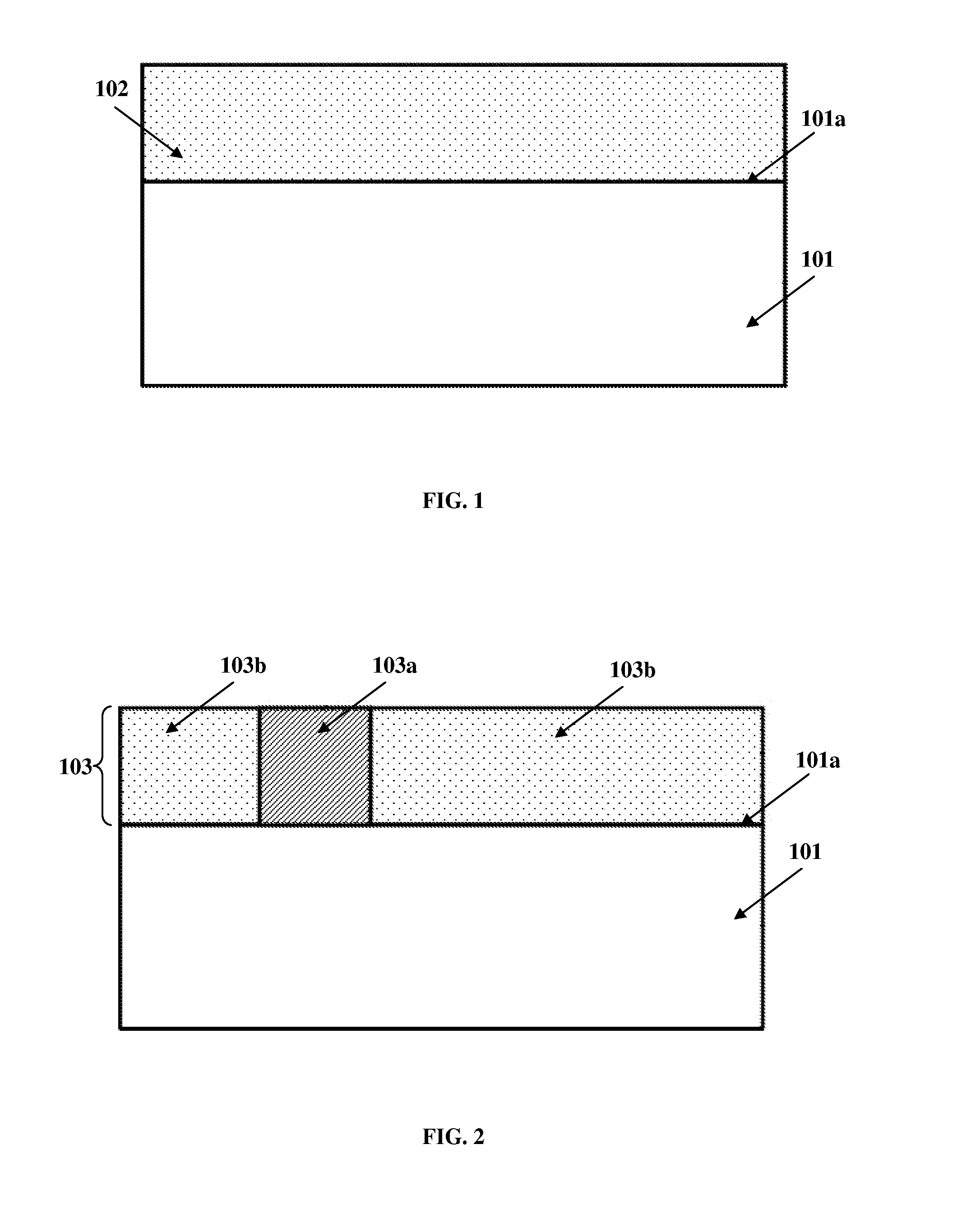
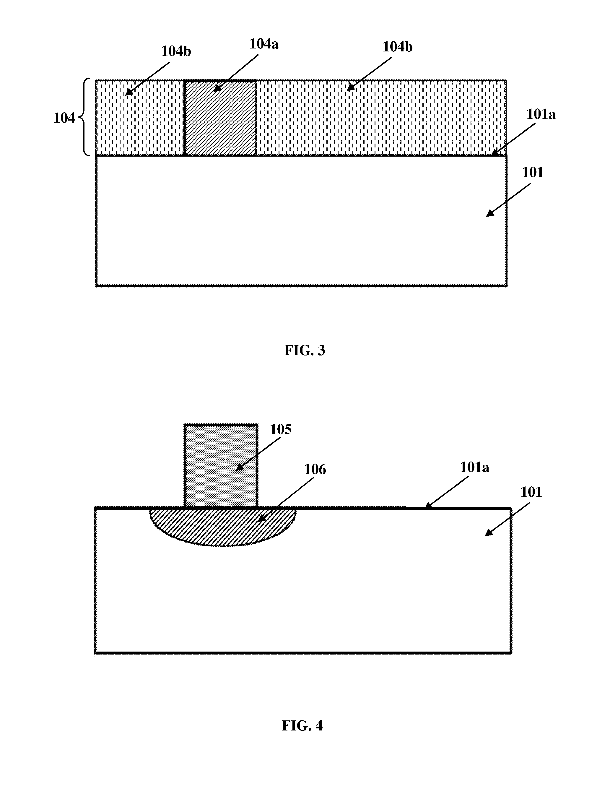
[0049]A doped liquid precursor is deposited on the substrate wafer 101 to create a doped polysilane film 102 on the surface 101a of the substrate wafer 101 as exemplarily illustrated in FIG. 1. The doped polysilane film 102 is selectively cured, for example, with ultraviolet light, to create a selectively cured doped polysilane film 103 comprising cured regions 103a and uncured regions 103b as exemplarily illustrated in FIG. 2. The selectively cured doped polysilane film 103 is selectively oxidized to create a selectively oxidized doped polysilane film 104 comprising oxidized uncured regions 104b and a non-oxidized cured region 104a as exemplarily illustrated in FIG. 3. The oxidized uncured regions 104b are removed. The non-oxidized cured region 104a of the selectively oxidized doped polysilane film 104 is heated to diffuse the dopants into the substrate wafer 101 to create a heavily diffused region 106 in the substrate wafer 101 as exemplarily illustrated in FIGS. 4-8. Subsequently...


PUM


Abstract

Methods for selectively diffusing dopants into a substrate wafer are provided. A liquid precursor is doped with dopants. The liquid precursor is selected from a group comprising monomers, polymers, and oligomers of silicon and hydrogen. The doped liquid precursor is deposited on a surface of the substrate wafer to create a doped film. The doped film is heated on the substrate wafer for diffusing the dopants from the doped film into the substrate wafer at different diffusion rates to create a heavily diffused region and a lightly diffused region in the substrate wafer. The method disclosed herein further comprises selective curing of the doped film on the surface of the substrate wafer. The selectively cured doped film acts as a diffusion source for selectively diffusing the dopants into the substrate wafer.

Description

BACKGROUND[0001]The method disclosed herein, in general, relates to a process for doping the surface of a solar cell. More particularly, the method disclosed herein relates to a use of a doped film on the surface of the solar cell as a diffusion source.[0002]Typical solar cells are made on p-type silicon wafers with n-type diffusion on a front surface to form a p-n junction. The diffused region is called an emitter, and is usually formed by phosphorus diffusion. The emitter is doped heavily in order to form one or more metal contacts as well as to obtain a low sheet resistance. Silver paste is typically used to provide a metal contact. The silver paste penetrates into the emitter when the silicon wafer is heat treated. Doping of the emitter region needs to be thick to contain the silver within the emitter region and not allow the silver to penetrate into a depletion region or a p-type region. The practical requirements of the heavy phosphorous doping in the emitter region suffer fro...

Claims


Application Information

Patent Timeline
IPC IPC(8): H01L21/225H01L31/18
CPCH01L21/2225H01L21/2255H01L21/228H01L31/1804Y02E10/547H01L31/068Y02E10/546
Inventor INNS, DANIEL
Owner CHEMTRON RES
Why Eureka
Try Eureka