RF Amplifier with Digital Filter for Polar Transmitter

a technology of polar transmitter and digital filter, applied in the direction of digital transmission, amplifier combination, gated amplifier, etc., can solve the problems of inacceptable spectral power emission, limited conventional power supply modulation techniques for many wideband applications, and several challenges for polar transmitters

Active Publication Date: 2012-03-08
TELEFON AB LM ERICSSON (PUBL)
View PDF19 Cites 22 Cited by
  • Summary
  • Abstract
  • Description
  • Claims
  • Application Information

AI Technical Summary

Benefits of technology

[0012]Embodiments of the invention can have any other features added, some such add

Problems solved by technology

In addition, polar transmitters also have several challenges related to amplitude modulation and power control.
Therefore, conventional power supply modulation techniques are limited for many wideband applications.
Any distortion leads to unacceptable spectral power emissions (“spectral leakage” or “spectral regrowth”) in neighbouring transmit channels.
As a result, the leakage covers the RF

Method used


Image

  • RF Amplifier with Digital Filter for Polar Transmitter
  • RF Amplifier with Digital Filter for Polar Transmitter
  • RF Amplifier with Digital Filter for Polar Transmitter

Examples


first embodiment

FIG. 1, a First Embodiment

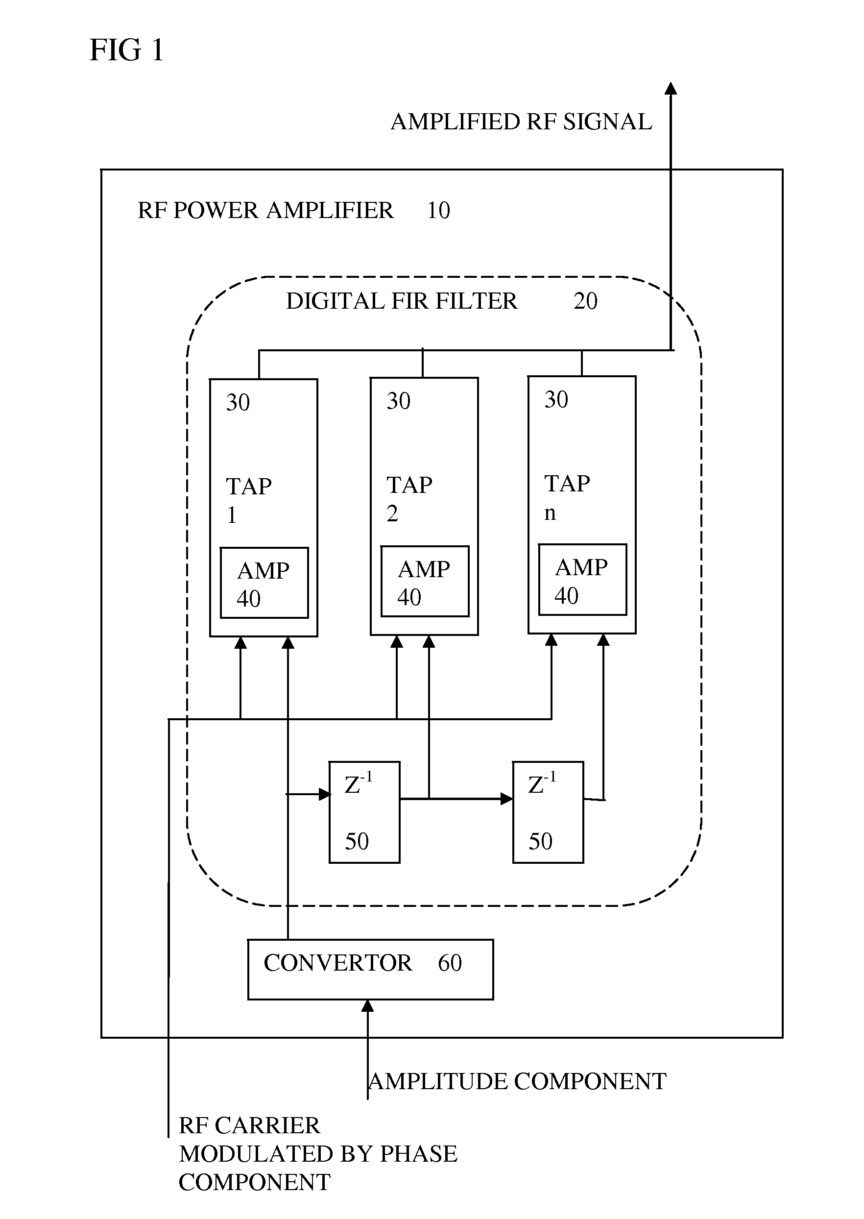
[0041]In the embodiment of FIG. 1, an RF power amplifier 10 is shown having a converter 60 and a digital finite impulse response FIR filter 20. The converter converts the amplitude component signal into a 1-bit digital amplitude signal, which is fed to the digital finite impulse response filter. The filter has a number of delay elements 50 which provide successively delayed versions of the amplitude signal to successive taps 30 of the filter. Three taps are shown, but there can be many more. Each tap has an RF amplification stage 40 arranged to amplify the delayed versions of the 1-bit digital amplitude signal, the amplifying being according to a respective tap coefficient. Each amplification stage also has an input of an RF carrier modulated by the phase component. The filter is arranged to combine the outputs of the taps to provide the amplified RF signal. This can be fed to an antenna, or waveguide, or any transmission medium. The modulation of the RF ca...

second embodiment

FIG. 2, a Second Embodiment

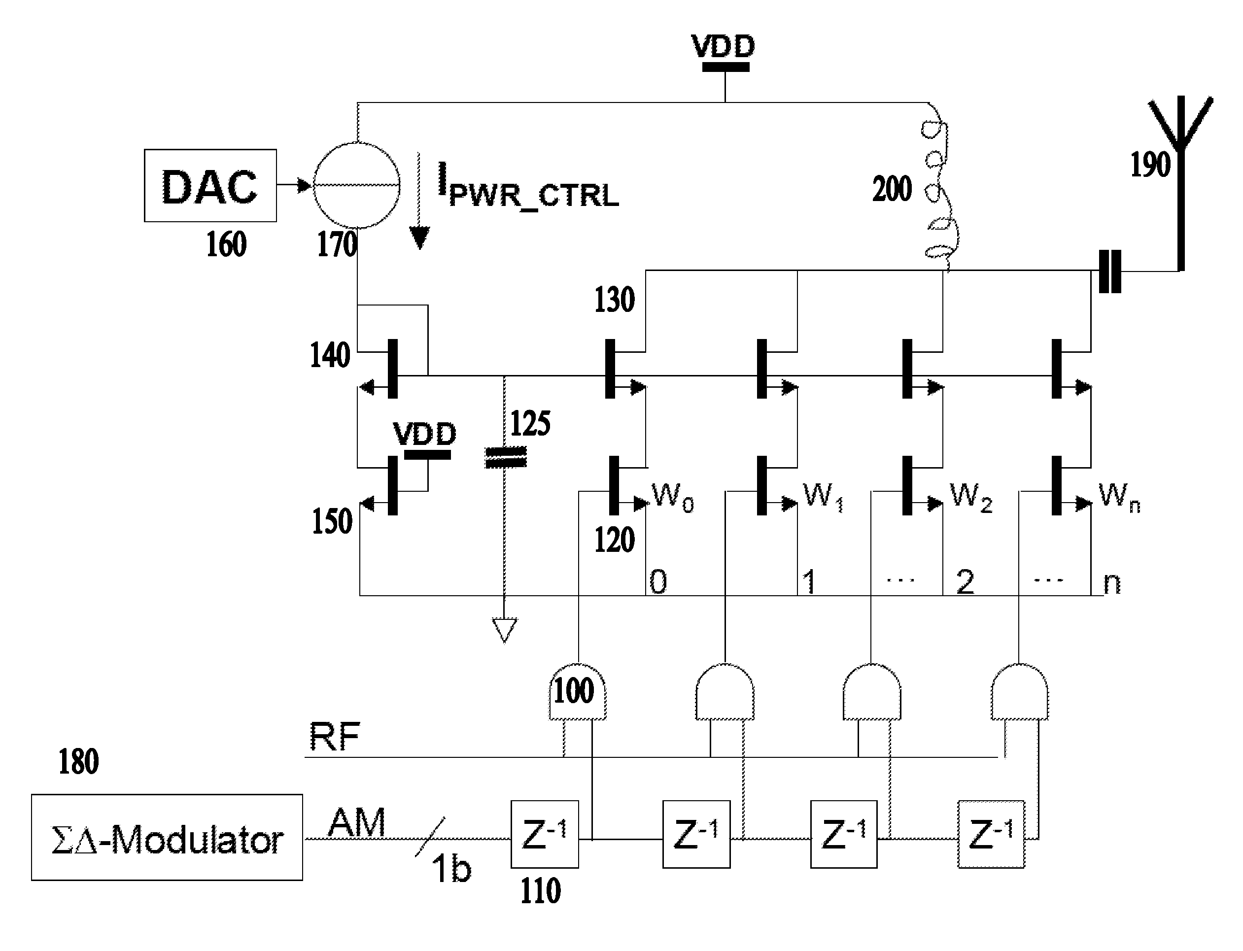
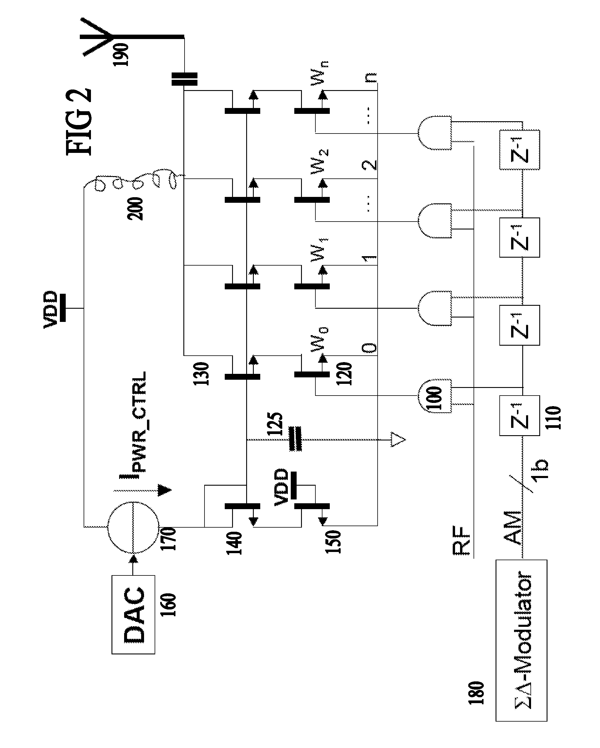
[0043]This figure shows an RF power amplifier having a digital FIR of N unit cells, the taps of a Nth-order FIR filter. Each unit cell consists of a delay element Z−1 110 (e.g. implemented with a flip-flop), a gate such as an AND gate 100, and an amplifying stage in the form of an RF switch NMOS transistor (bottom NMOS 120) and a Cascode NMOS (top NMOS 130). The drains of the Cascodes of the N unit cells are combined and connected to the antenna 190. The digital AM signal is converted to a 1-bit digital signal by a converter in the form of a Sigma Delta Modulator 180. The AND gates combine the AM bit-stream and the RF carrier. The RF switch transistors 120 have weights W0 . . . Wn, as per the required tap coefficients weights to constitute the desired filter response. The weighting is achieved by using different dimensions for the switch transistors of different taps. The diode connected NMOS 140 on the left and dummy RF transistor 150, provide a relativel...

third embodiment

FIG. 3, a Third Embodiment

[0045]In the embodiment of FIG. 3, some parts are similar to FIG. 2 and corresponding reference signs are used as appropriate. Each unit PA cell consists of a delay element, an AND gate, an RF switch transistor and a current mirror, doubling as the Cascode transistor. Unlike FIG. 2, all unit cells have the same dimensions W for the transistors. The weight of the FIR filter tap coefficient is no longer determined by the dimensions, but instead is determined by the DC current provided by individual current sources 165 into each unit mirror. In this embodiment since all RF transistors have the same dimensions, there is good matching of RF characteristics and easier design of the layout. The matching of the tap coefficients is determined by DC transistors (the current sources I0 . . . In, 165) can have a large size (since there are no RF constraints, only DC).

[0046]Power control is achieved by controlling a common reference current to alter the full scale curre...


PUM


Abstract

An RF power amplifier for a polar transmitter converts an amplitude component signal into a 1-bit digital amplitude signal, which is fed to a digital finite impulse response filter. Successive taps of the filter each have an RF amplification stage arranged to amplify successively delayed versions of the 1-bit digital amplitude signal, the amplifying being according to a respective tap coefficient, and according to the RF carrier modulated by the phase component. The filter is arranged to combine the outputs of the taps to provide the amplified RF signal. The power amplifier uses a one bit stream which therefore has only two states (2 values), thus achieving linearity in principle. Device mismatch between taps does not lead to non-linearity or distortion.

Description

FIELD OF THE INVENTION[0001]This invention relates to power amplifiers especially RF power amplifiers, and corresponding transmitters, transceivers, integrated circuits and methods of operating the same.BACKGROUND OF THE INVENTION[0002]It is known from US 2007275676 that modern wireless RF transmitters for applications such as cellular, personal, and satellite communications, employ digital modulation schemes, such as frequency shift keying (FSK), phase shift keying (PSK), and variants thereof, often in combination with code division multiple access (CDMA) communication. The RF transmitter output signal will have an envelope which in some of the above mentioned communication schemes is a constant envelope, and in other communications schemes will vary with time. An example of a variable-envelope modulation scheme is that known as a polar transmitter. In a polar transmitter, digital baseband data enters a digital processor that performs the necessary pulse shaping and modulation to s...

Claims


Application Information

Patent Timeline
IPC IPC(8): H03F3/68H03F1/22
CPCH03F3/193H03F3/211H03F3/245H03F2203/21112H03F3/72H03F2203/21157H04L27/361H03F3/2178H03F2203/21145
Inventor FRAMBACH, JOHANNES PETRUS ANTONIUS
Owner TELEFON AB LM ERICSSON (PUBL)
Why Eureka
Try Eureka