

Semiconductor device
a technology of semiconductor devices and dielectric breakdowns, applied in the direction of semiconductor devices, transistors, electrical equipment, etc., can solve the problems of destroying the ldmos transistor by dielectric breakdown between the source and the drain, increasing the current which cannot be controlled by the gate electrode b>55/b>, and not achieving sufficient esd toleran
- Summary
- Abstract
- Description
- Claims
- Application Information
AI Technical Summary
Benefits of technology
Problems solved by technology
Method used
Image

Examples
Embodiment Construction
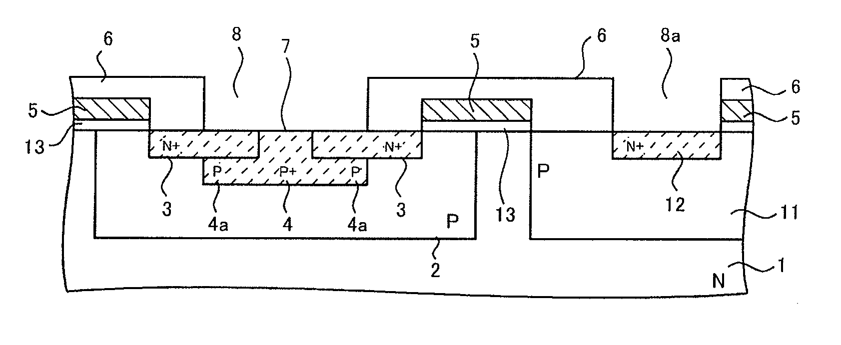
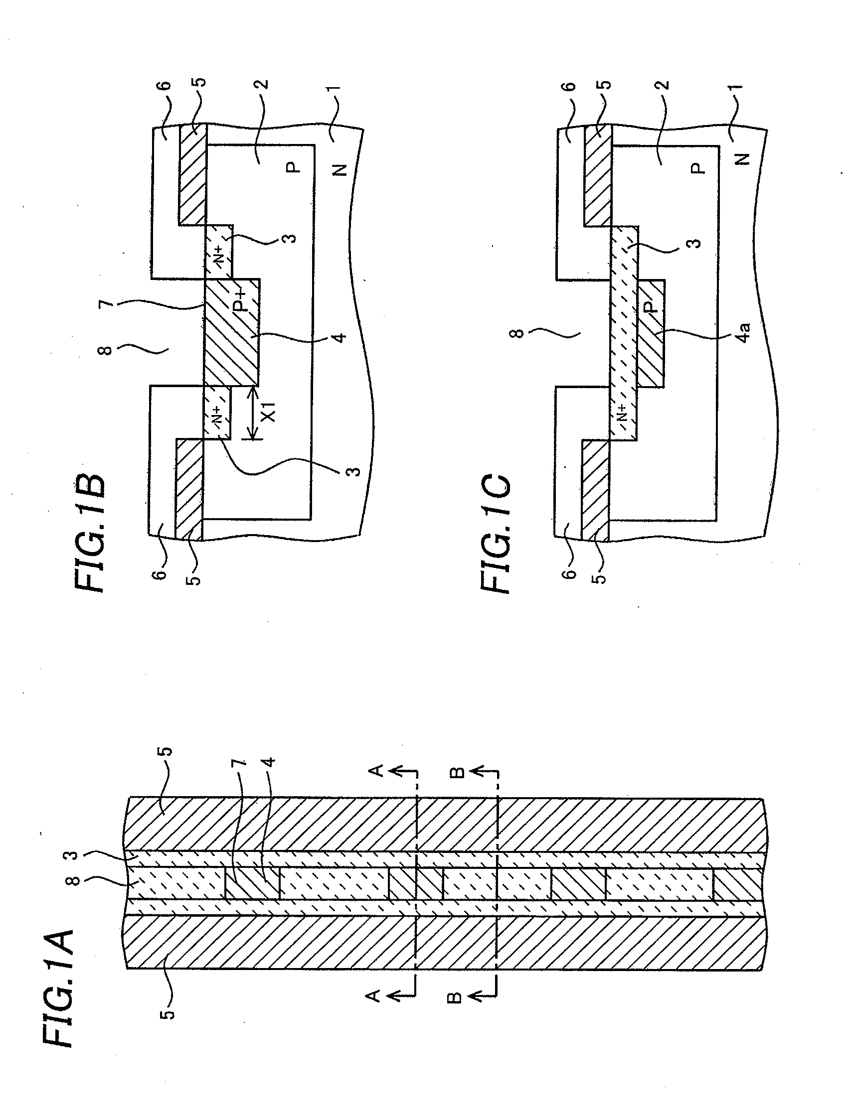
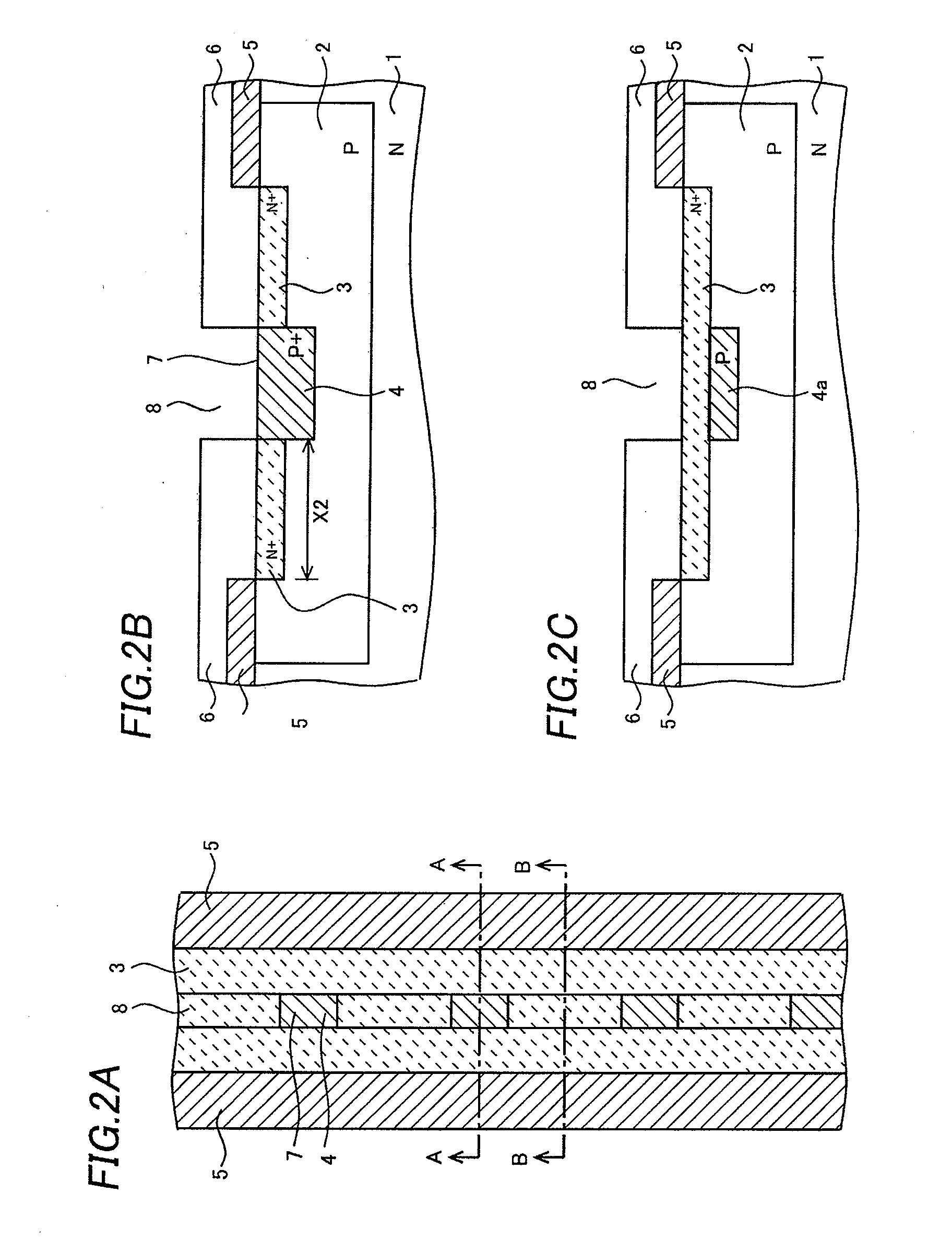
[0046]LDMOS transistors according to embodiments of this invention will be explained referring to FIG. 1A-FIG. 11C. In one of preferable embodiments, the transistor has the structure shown in FIGS. 3A, 3B and 3C, wherein a distance X3 shown in FIG. 3B is around 1.5 μm. This invention relates to increasing an area of an N+ type source layer 3, which is shaped in a ladder having a plurality of evenly spaced openings 7 in its center. Specifically, this invention relates to a correlation between a distance X from an edge of the opening 7, in which a P+ type contact layer 4 is buried, to an edge of the N+ type source layer 3 and an HBM ESD tolerance that increases and eventually saturates as the distance X increases. Therefore, a drain region is omitted from the drawings, and the explanation is given referring to simplified drawings in which a source region is represented by a single N+ type source layer 3. The N+ type source layer 3 is formed in a P type base layer 2. Gate electrode 5 i...
PUM
 Abstract
Description
Claims
Application Information