Light emitting and lasing semiconductor methods and devices
What is Al technical title?
Al technical title is built by PatSnap Al team. It summarizes the technical point description of the patent document.
a technology of semiconductors and semiconductor lasers, applied in semiconductor lasers, semiconductor devices, electrical apparatus, etc., can solve the problems of limited intrinsic high speed capability of devices, and achieve the effects of excellent devices for material study, small base recombination lifetime and fast recombination speed
Inactive Publication Date: 2012-03-22
QUANTUM ELECTRO OPTO SYST
View PDF4 Cites 22 Cited by
Summary
Abstract
Description
Claims
Application Information
AI Technical Summary
This helps you quickly interpret patents by identifying the three key elements:
Problems solved by technology
Method used
Benefits of technology
[0007]The transistor, a structure comprising an emitter, base and collector, can be an excellent device to use for material study. Emitter gain β, a metric of the ratio of the collector current Ic, to the base current, Ib (β=Ic / Ib), can also be given as the ratio of the base recombination time over the base transit time τB / τt. Therefore, for transistors of comparable junction characteristics, similar physical dimensions and base resistivity, a lower beta device usually indicates smaller (hence, faster) base recombination lifetime.
[0008]By using the transistor technique to study the recombination lifetime of a base material, Applicant found that the defect levels in a highly doped semiconductor material can be controlled through growth variations such as doping concentration, gas flow and growth temperature. By increasing the defect levels in a layer, the recombination speed of that layer increases, resulting in a device with much lower β. Applicant has also found that alloys such as AlGaAs are more prone to such decrease in recombination lifetime when compared to binary systems such as GaAs. (As will be treated hereinbelow, diffusion length for minority carriers in a semiconductor material is inversely related to defect concentration in the material.) Applicant also found that transistors with 13 as low as 0.01 (that is, 99% of minority carrier recombined within a single pass of the base region) could be achieved, indicating that a very fast non-radiative recombination material is possible via defect engineering. Importantly, the engineering of defects can be done without degrading the majority carrier electrical characteristics (resistivity) of the layer. This fast recombination characteristic indicates that an engineered high defect layer (or engineered short diffusion length layer) may be used as an effective secondary mechanism for collection / draining of excess minority carriers. Also, combinations one or more of engineered high defect concentration layers (short diffusion length layers) and one or more engineered low defect concentration layers (long diffusion length layers) in design of a tilted-charge light-emitting devices can provide substantial advantage.
[0010]A form of the invention is applicable for use in conjunction with a light-emitting semiconductor structure that includes a semiconductor active region of a first conductivity type containing a quantum size region and having a first surface adjacent a semiconductor input region of a second conductivity type that is operative, upon application of electrical potentials with respect to said active and input regions, to produce light emission from said active region. A method is provided for enhancing operation of said light-emitting semiconductor structure, comprising the following steps: providing a semiconductor output region that includes a semiconductor auxiliary layer of said first conductivity type adjacent a second surface, which opposes said first surface of said active region, and providing said auxiliary layer as comprising a semiconductor material having a diffusion length for minority carriers of said first conductivity type material that is substantially shorter than the diffusion length for minority carriers of the semiconductor material of said active region.
Problems solved by technology
The intrinsic high speed capability of the device is this limited by the time required to access to thus secondary mechanism, also known as the transit time, τt.
Method used
Image
Click on the blue label to locate the original text in one second.
Reading with bidirectional positioning of images and text.
Examples
Embodiment Construction
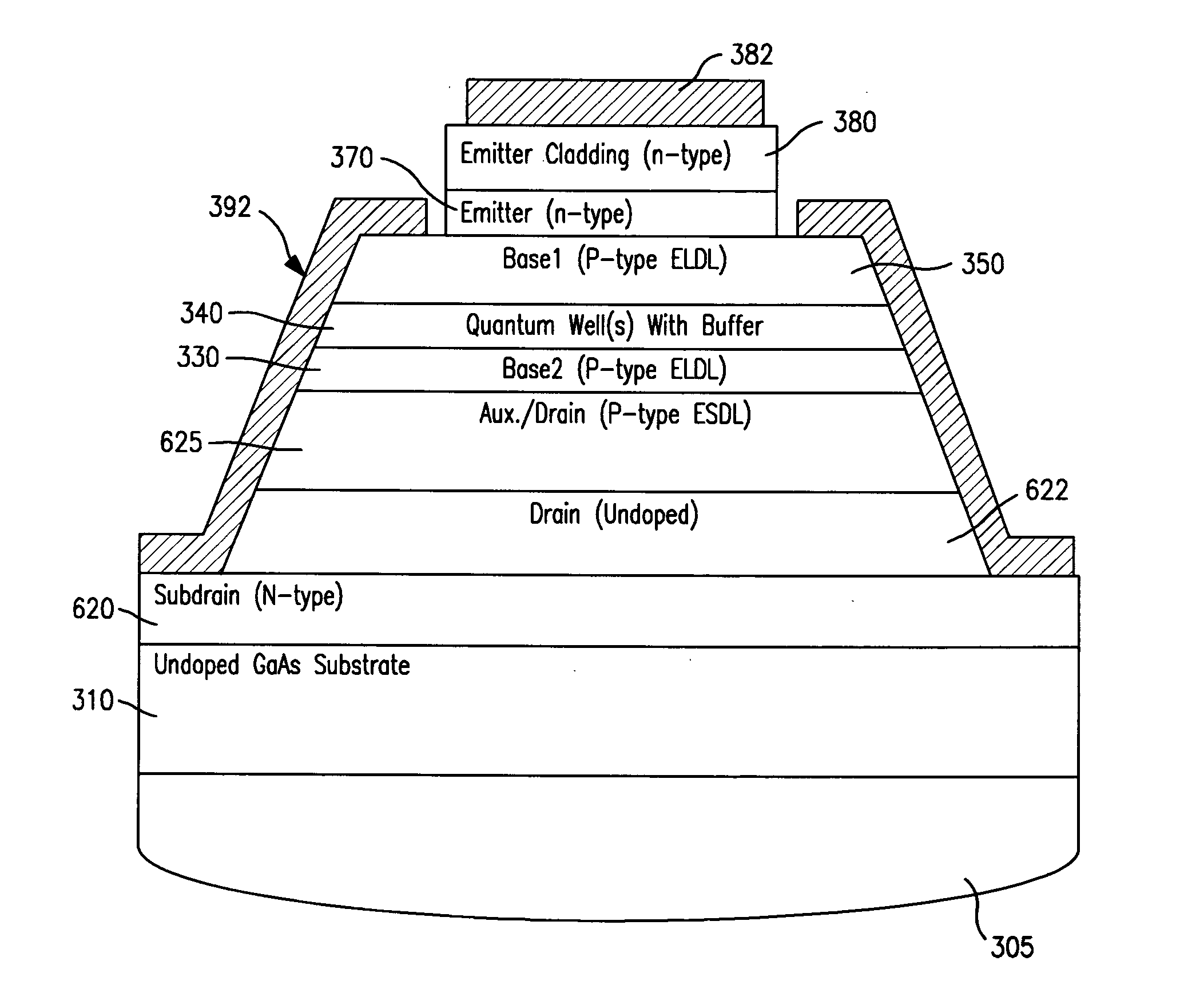
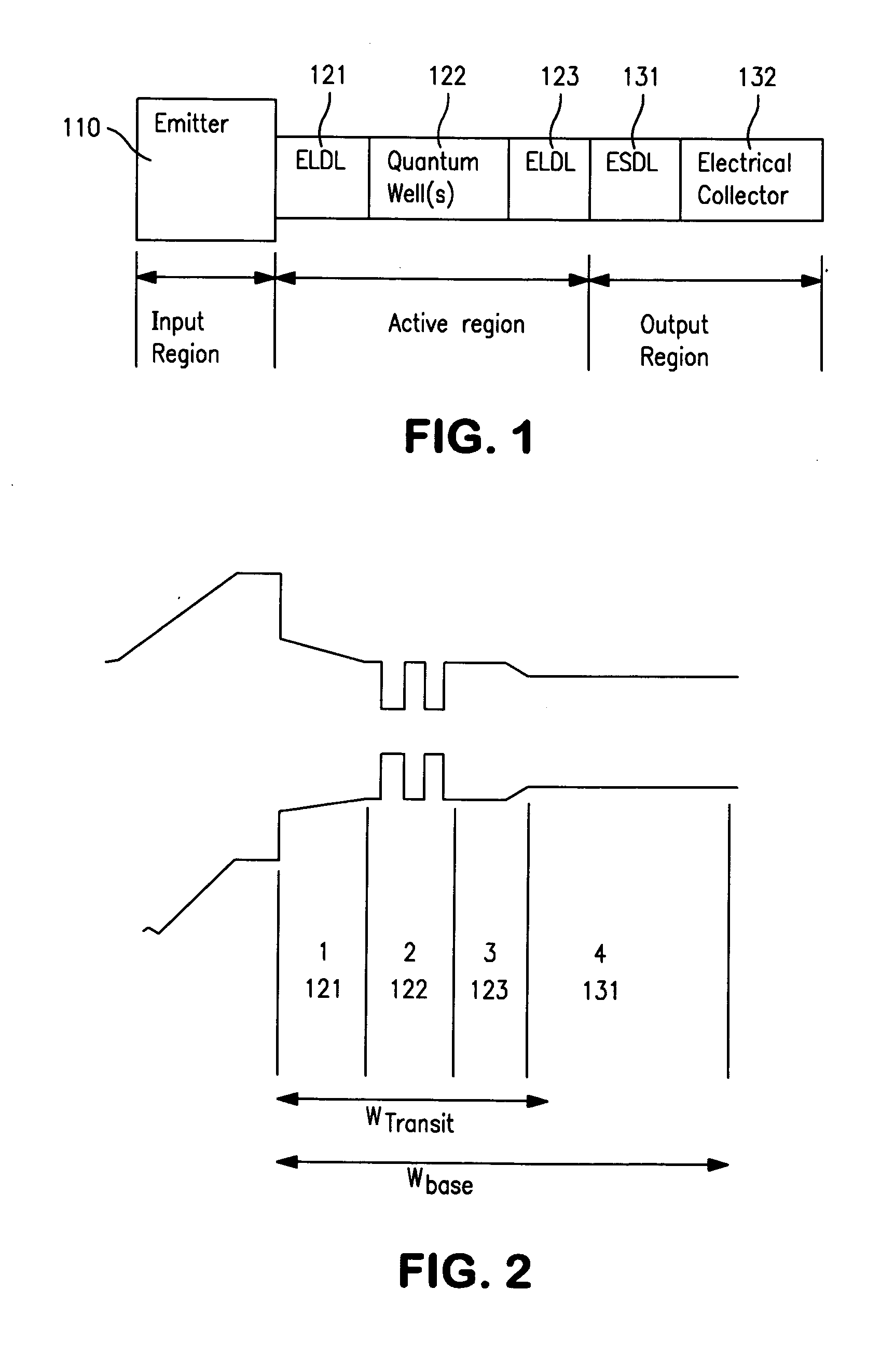
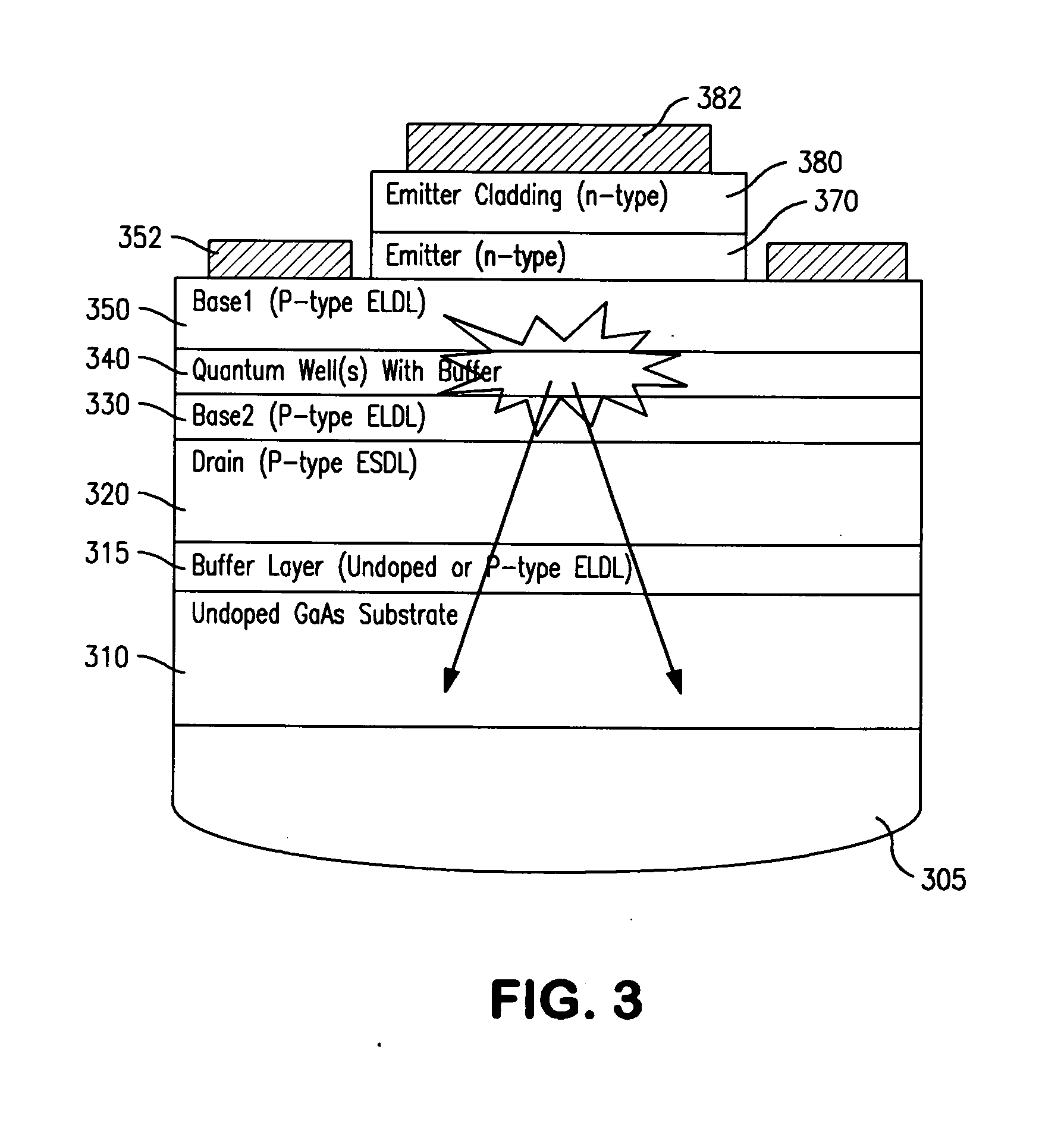
[0028]The diffusion length (L) of a minority carrier in the material of a semiconductor device is given as:
L=√{square root over (D×τ)}
where, D, is the diffusion coefficient, which depends on the carrier mobility in the semiconductor, and μ is expressed in:
D=μ×kTq
where q is the charge, T is temperature, and k is the Boltzmann constant. The carrier mobility, μ, is proportional to the average scattering time, which is dependent, among many factors, on doping concentrations, defect concentrations, and semiconductor material composition (for example, GaAs versus AlGaAs (binary vs. alloy), or GaAs vs. InP (different material systems)). The minority carrier lifetime, τ, is also dependent, among other factors, on free carrier concentrations (related to doping concentrations), defect energy levels, and defect concentration. In regions of short minority carrier diffusion lengths, minority carriers have higher probability of recombining with majority carriers per unit distance.
[0029]A tilted-c...
PUM
Abstract
The invention is applicable for use in conjunction with a light-emitting semiconductor structure that includes a semiconductor active region of a first conductivity type containing a quantum size region and having a first surface adjacent a semiconductor input region of a second conductivity type that is operative, upon application of electrical potentials with respect to the active and input regions, to produce light emission from the active region. A method is provided that includes the following steps: providing a semiconductor output region that includes a semiconductor auxiliary layer of the first conductivity type adjacent a second surface, which opposes the first surface of the active region, and providing the auxiliary layer as a semiconductor material having a diffusion length for minority carriers of the first conductivity type material that is substantially shorter than the diffusion length for minority carriers of the semiconductor material of the active region.
Description
PRIORITY CLAIM[0001]Priority is claimed from U.S. Provisional Patent Application No. 61 / 403,748, filed Sep. 21, 2010, and said U.S. Provisional Patent Application is incorporated herein by reference.FIELD OF THE INVENTION[0002]This invention relates to methods and devices for producing light emission and laser emission in response to electrical signals. The invention also relates to methods and devices for producing light emission and laser emission from semiconductor devices with improved efficiency and speed, and to increasing light output from semiconductor light-emitting devices.BACKGROUND OF THE INVENTION[0003]A part of the background hereof lies in the development of heterojunction bipolar transistors which operate as light-emitting transistors and transistor lasers. Reference can be made, for example, to U.S. Pat. Nos. 7,091,082, 7,286,583, 7,354,780, 7,535,034 and 7,693,195; U.S. Patent Application Publication Numbers US2005 / 0040432, US2005 / 0054172, US2008 / 0240173, US2009 / 01...
Claims
Application Information
Patent Timeline
Application Date:The date an application was filed.
Publication Date:The date a patent or application was officially published.
First Publication Date:The earliest publication date of a patent with the same application number.
Issue Date:Publication date of the patent grant document.
PCT Entry Date:The Entry date of PCT National Phase.
Estimated Expiry Date:The statutory expiry date of a patent right according to the Patent Law, and it is the longest term of protection that the patent right can achieve without the termination of the patent right due to other reasons(Term extension factor has been taken into account ).
Invalid Date:Actual expiry date is based on effective date or publication date of legal transaction data of invalid patent.
Patent Type & Authority Applications(United States)