Method of making oxide thin film transistor array, and device incorporating the same

a transistor array and thin film technology, applied in the direction of transistors, semiconductor devices, electrical devices, etc., can solve the problems of restricting the types of materials that can be used as substrates, and achieve the effect of increasing the conductivity of the substra

Inactive Publication Date: 2012-03-29
GUARDIAN GLASS LLC
View PDF9 Cites 41 Cited by
  • Summary
  • Abstract
  • Description
  • Claims
  • Application Information

AI Technical Summary

Benefits of technology

[0017]Certain example embodiments of this invention relate to an electronic device including a TFT substrate. The TFT substrate comprises a soda lime glass substrate (e.g., as opposed to a borosilicate glass substrate, which may be used in different embodiments of this invention). A silicon-inclusive barrier layer is sputter deposited at low or room temperature, directly or indirectly, on the soda lime glass substrate (e.g., to help reduce and sometimes even eliminate the migration of sodium from the glass substrate into one or more of the thin film and / or other layers on the substrate). An oxide semiconductor layer comprising IGZO, amorphous or polycrystalline ZnO, ZnSnO, or InZnO, is sputter deposited at low or room temperature, directly or indirectly, on the barrier layer. A gate insulator layer is sputter deposited at low or room temperature, directly or indirectly, on the oxide semiconductor layer. A gate metal layer is sputter deposited at low or room temperature, directly or indirectly, on the gate insulator layer. One or more portions of the gate insulator layer and the gate metal layer are removed to expose the underlying oxide semiconductor layer. One or more portions of the oxide semiconductor layer are removed to create at least one island, the at least one island being plasma treated so as to increase the conductivity thereof. A passivation layer is deposited atop the barrier layer, the at least one island, and the gate insulator layer, the passivation layer being patterned to form source and drain contact holes. Source and drain lines are deposited over at least a portion of the passivation layer and in the source and drain contact holes.

Problems solved by technology

In addition, the high temperatures involved in current techniques restrict the types of materials that can be used as the substrates.

Method used


Image

  • Method of making oxide thin film transistor array, and device incorporating the same
  • Method of making oxide thin film transistor array, and device incorporating the same
  • Method of making oxide thin film transistor array, and device incorporating the same

Examples


Embodiment Construction

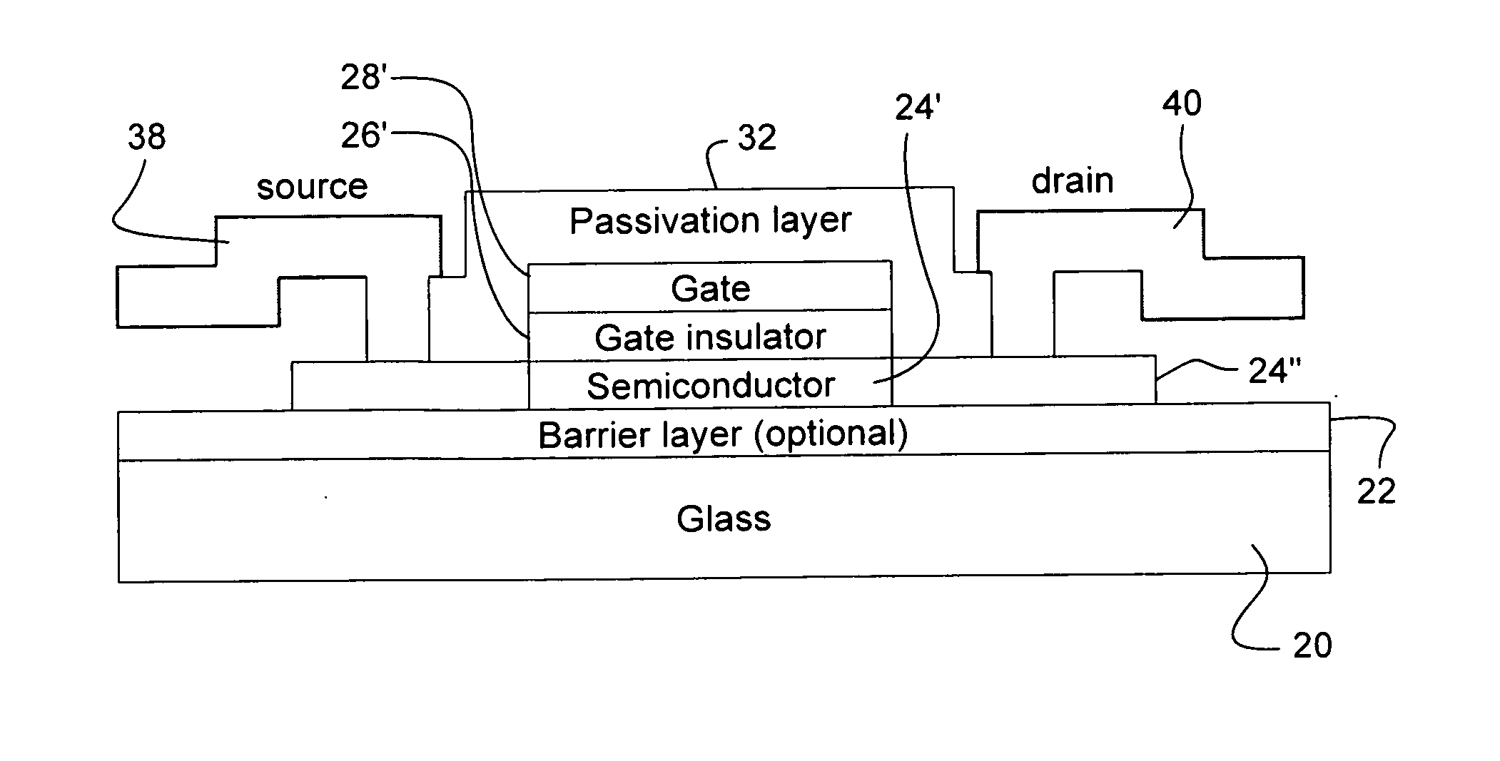
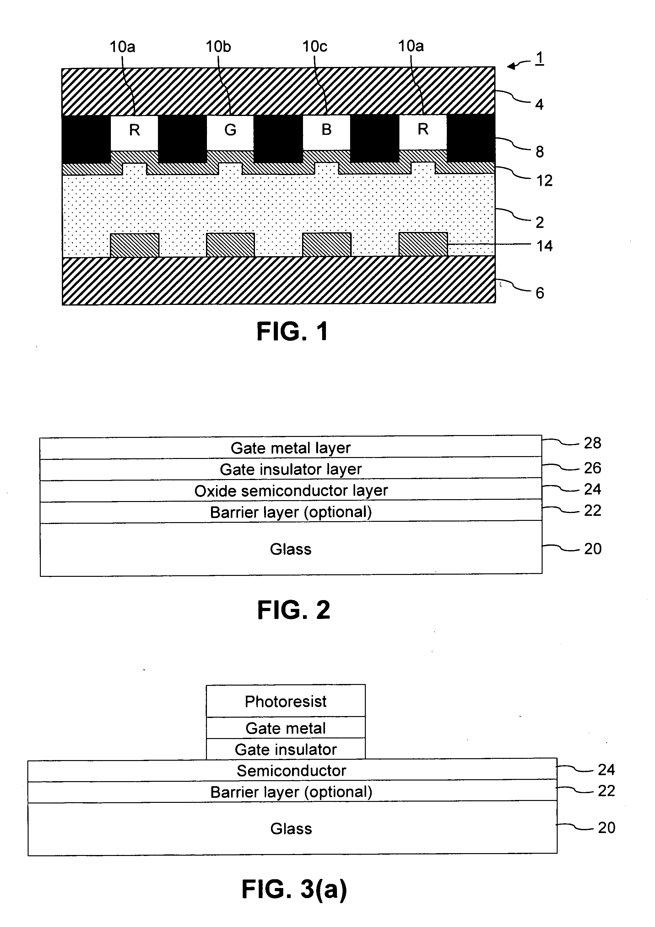
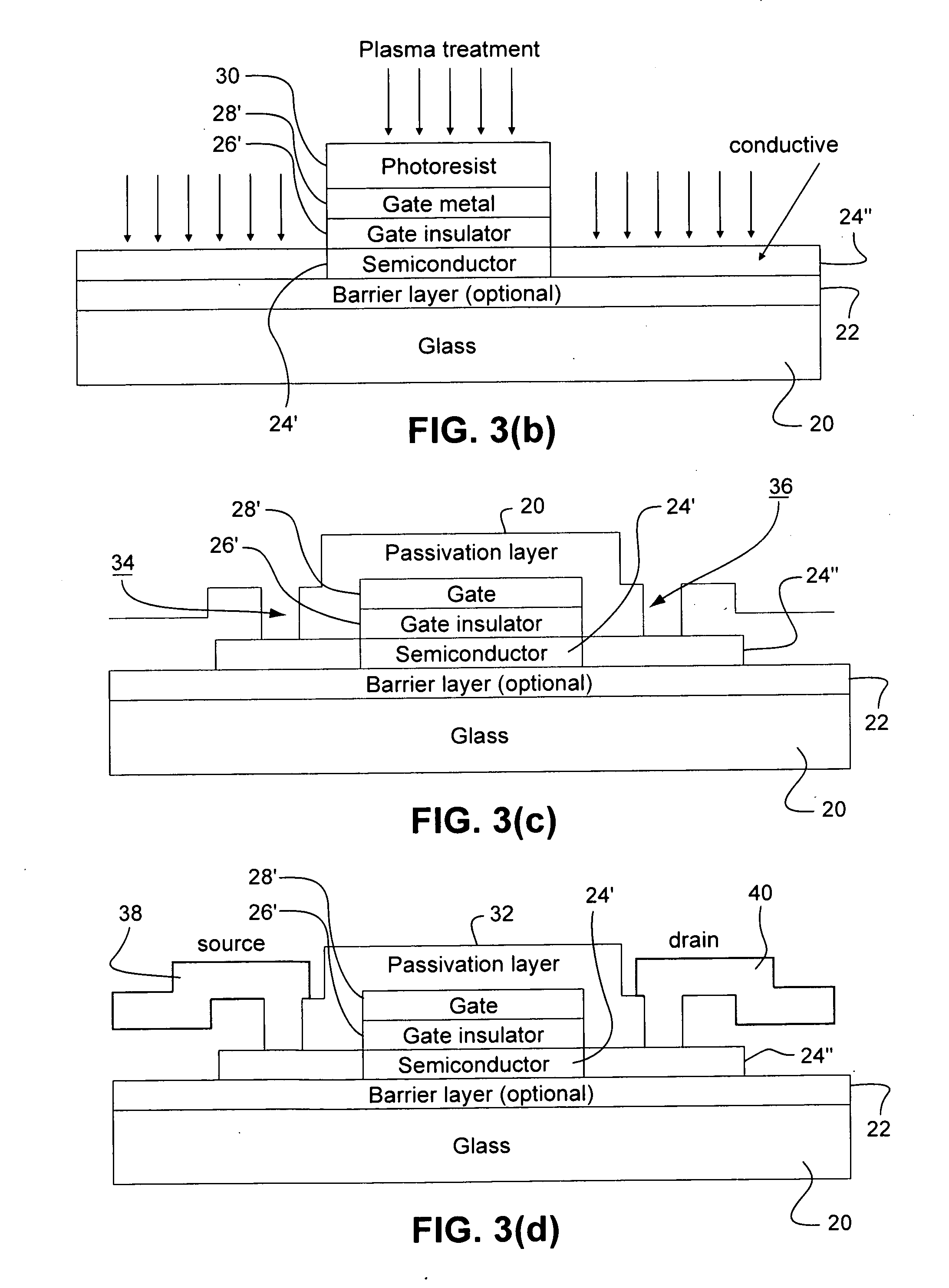
[0024]Certain example embodiments relate to complex oxide-based thin film transistors (TFTs) on glass substrates for flat panel displays and the like. In certain example embodiments, the barrier layer, semiconductor layer, gate insulator layer and, optionally, gate metal layer, may be sequentially deposited as blanket layers, e.g., by low or room temperature sputtering prior to any patterning steps for the TFT substrate. These layers for the TFT array therefore may be deposited cost-effectively in large area inline coaters. The layer stacks deposited on the glass add value to the glass substrate, and the example process flows described herein may reduce and sometimes even eliminate the need for customers, such as LCD manufacturers, to invest in, operate, and maintain PECVD equipment for semiconductor and gate insulator deposition.

[0025]As indicated above, some a-Si TFT arrays for LCD TVs, monitors, notebook displays, etc., are fabricated by first depositing and patterning a gate met...


PUM

PropertyMeasurementUnit
threshold voltageaaaaaaaaaa
thicknessaaaaaaaaaa
thicknessaaaaaaaaaa

Abstract

Certain example embodiments relate to methods of making oxide thin film transistor arrays (e.g., IGZO, amorphous or polycrystalline ZnO, ZnSnO, InZnO, and/or the like), and devices incorporating the same. Blanket layers of an optional barrier layer, semiconductor, gate insulator, and/or gate metal are disposed on a substrate. These and/or other layers may be deposited on a soda lime or borosilicate substrate via low or room temperature sputtering. These layers may be later patterned and/or further processed in making a TFT array according to certain example embodiments. In certain example embodiments, all or substantially all TFT processing may take place at a low temperature, e.g., at or below 150 degrees C., until a post-annealing activation step, and the post-anneal step may take place at a relatively low temperature (e.g., 200-250 degrees C.).

Description

FIELD OF THE INVENTION[0001]Certain example embodiments of this invention relate to methods of making oxide thin film transistor arrays, and devices incorporating the same. More particularly, certain example embodiments of this invention relate to oxide (e.g., IGZO) thin film transistor (TFT) arrays deposited using low or room temperature sputtering, and / or methods of making the same. In certain example embodiments, blanket layers of an optional barrier layer, semiconductor, gate insulator, and / or gate metal are disposed on a substrate. These layers may be later patterned and / or further processed in making a TFT array according to certain example embodiments.BACKGROUND AND SUMMARY OF EXAMPLE EMBODIMENTS OF THE INVENTION[0002]LCD devices are known in the art. See, for example, U.S. Pat. Nos. 7,602,360; 7,408,606; 6,356,335; 6,016,178; and 5,598,285, each of which is hereby incorporated herein in its entirety.[0003]FIG. 1 is a cross-sectional view of a typical LCD display device 1. Th...

Claims


Application Information

Patent Timeline
Patent Type & Authority Applications(United States)
IPC IPC(8): H01L29/786H01L33/08H01L33/58H01L33/28
CPCH01L29/78603H01L29/66969H01L29/7869H01L27/1225H01L29/66742H01L29/78618
Inventor DEN BOER, WILLEM
Owner GUARDIAN GLASS LLC
Why Eureka
Try Eureka