3D memory array with vertical transistor

a technology of memory array and transistor, which is applied in the direction of transistors, semiconductor devices, electrical equipment, etc., can solve the problems of limiting the size of switching devices, the size of memory cells is the limit factor in achieving greater areal densities, and the difficulty of forming the pillar structure of vertical transistors, etc., to achieve high density and high fill factor memory devices.

Inactive Publication Date: 2012-03-29
SEAGATE TECH LLC
View PDF2 Cites 224 Cited by
  • Summary
  • Abstract
  • Description
  • Claims
  • Application Information

AI Technical Summary

Benefits of technology

[0006]The present disclosure relates to a memory array that includes a plurality of memory array layers that are stacked on a base circuitry layer and individually controlled by the single base circuitry layer. In particular, the memory array that includes a plurality of memory array layers that includes a plurality of memory units where each memory unit includes a vertical pillar transistor electrically coupled to a STRAM or RRAM memory cell. The resulting 3D stacked memory array is a high density and high fill factor memory device.

Problems solved by technology

While operable, a limitation with the use of MOSFETs and other types of switching devices in a memory cell is the areal extent (size) of such devices.
Since this is significantly larger than the areal size of many types of memory elements, the switching device size can be a limiting factor in achieving greater areal densities in a memory array.
While advantageously promoting an enhanced areal data density, it can be difficult to form the pillar structure of the vertical transistor so that the transistor can operate optimally.

Method used


Image

  • 3D memory array with vertical transistor
  • 3D memory array with vertical transistor
  • 3D memory array with vertical transistor

Examples


Embodiment Construction

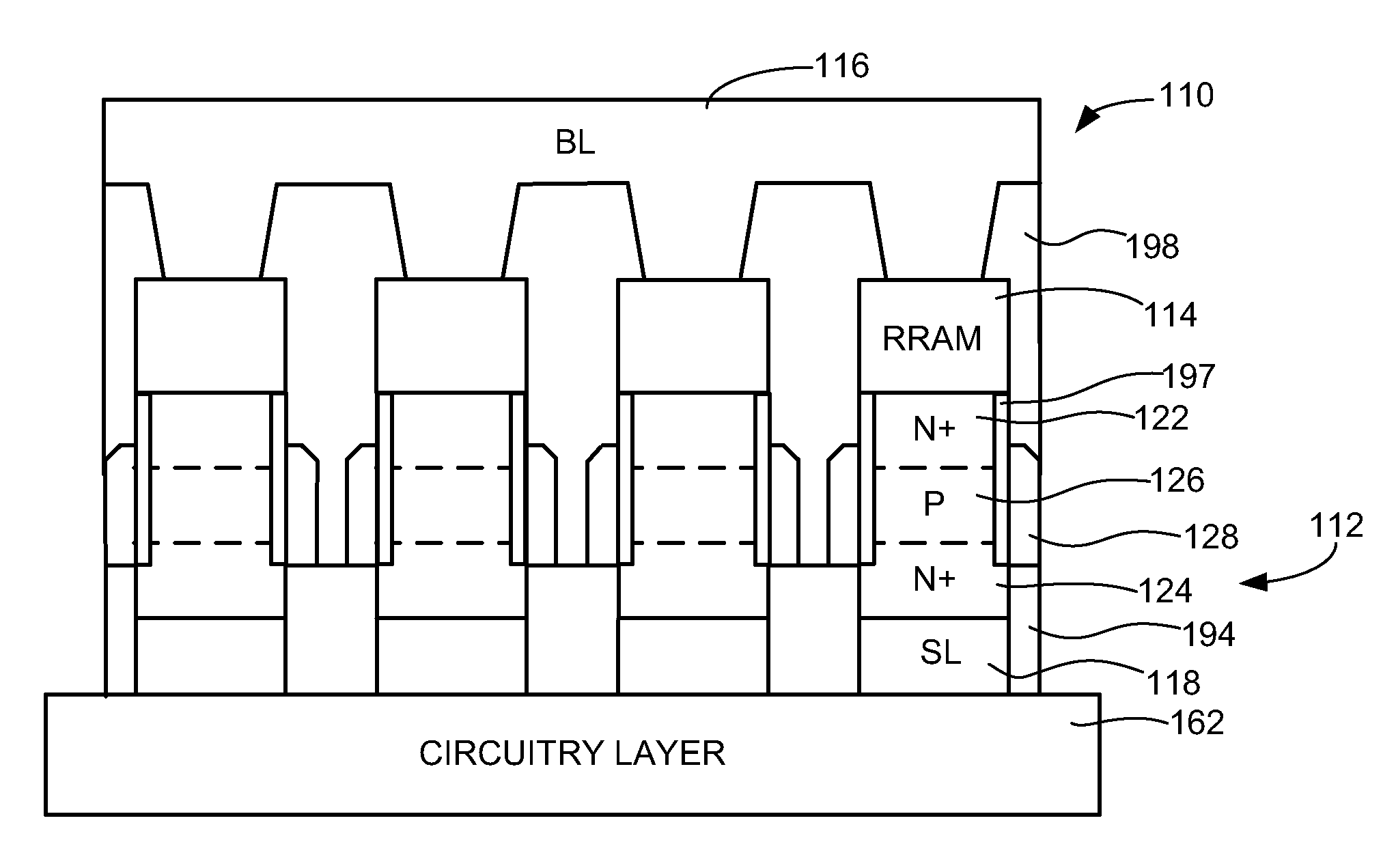
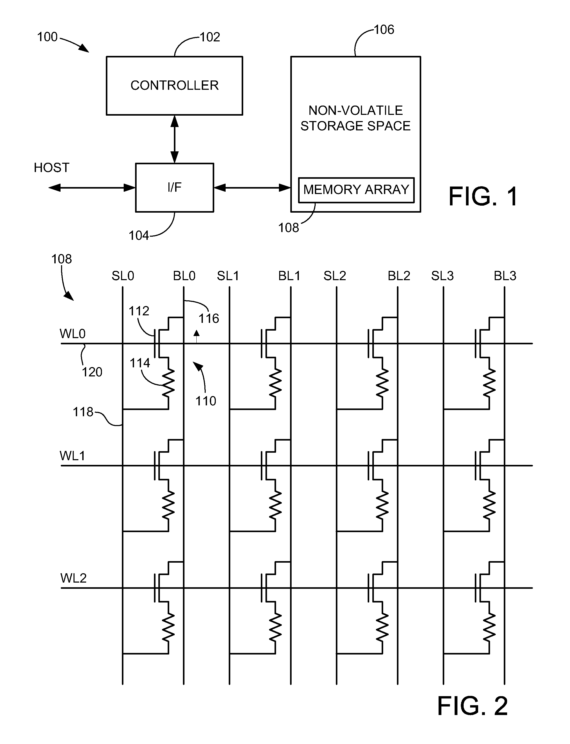
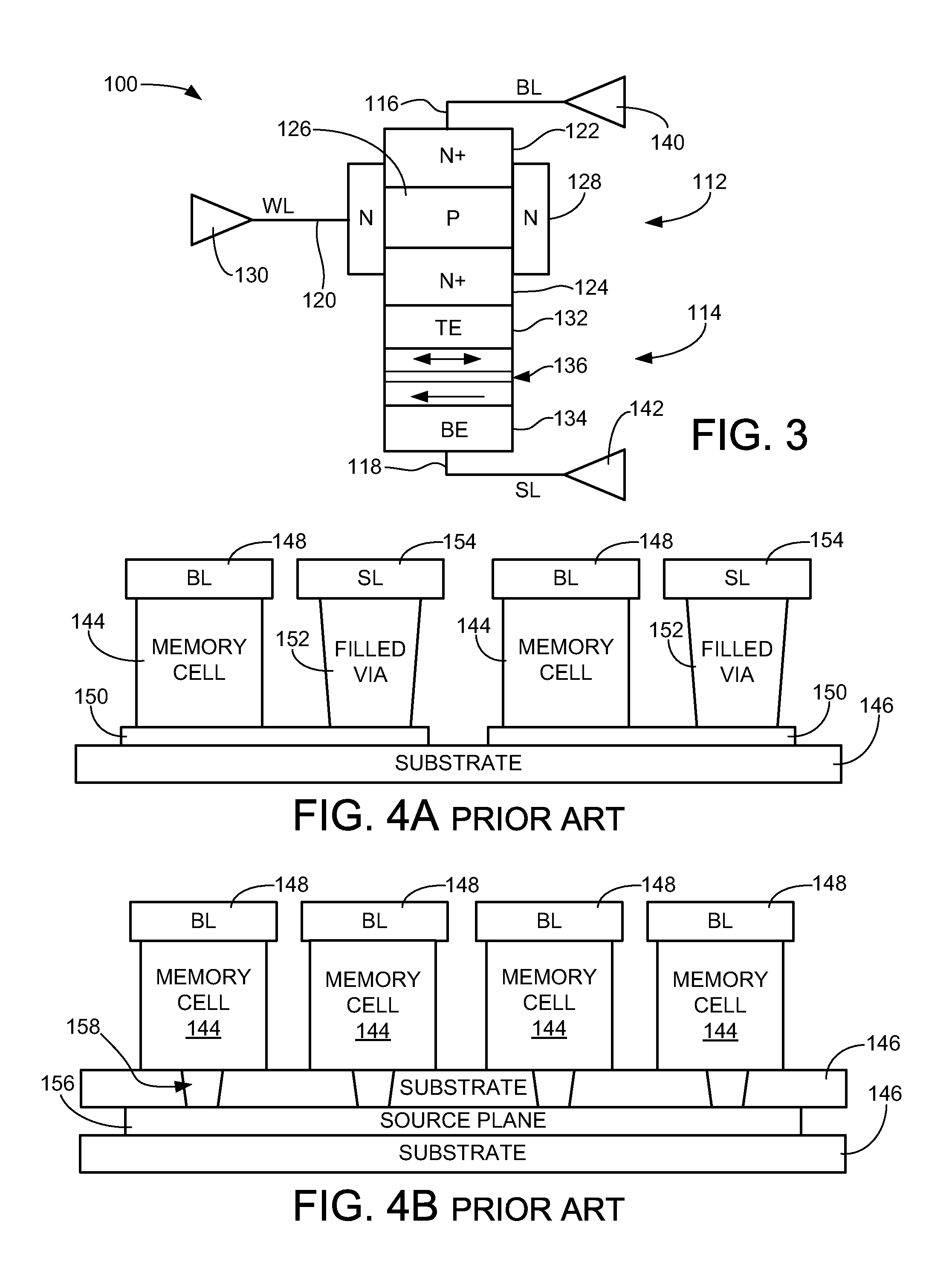
[0032]In the following description, reference is made to the accompanying set of drawings that form a part hereof and in which are shown by way of illustration several specific embodiments. It is to be understood that other embodiments are contemplated and may be made without departing from the scope or spirit of the present disclosure. The following detailed description, therefore, is not to be taken in a limiting sense. The definitions provided herein are to facilitate understanding of certain terms used frequently herein and are not meant to limit the scope of the present disclosure.

[0033]Unless otherwise indicated, all numbers expressing feature sizes, amounts, and physical properties used in the specification and claims are to be understood as being modified in all instances by the term “about.” Accordingly, unless indicated to the contrary, the numerical parameters set forth in the foregoing specification and attached claims are approximations that can vary depending upon the ...


PUM


Abstract

A memory array includes a base circuitry layer and a plurality of memory array layers stacked sequentially to form the memory array. Each memory array layer is electrically coupled to the base circuitry layer. Each memory array layer includes a plurality of memory units. Each memory unit includes a vertical pillar transistor electrically coupled to a memory cell.

Description

BACKGROUND[0001]Solid state memories (SSMs) provide an efficient mechanism for storing and transferring data in a wide variety of applications, such as hand-held portable electronic devices. Individual memory cells within such memories can be volatile or non-volatile, and can store data by the application of suitable write currents to the cells to store a sequence of bits. The stored bits can be subsequently read during a read access operation by applying suitable read currents and sensing voltage drops across the cells.[0002]Some SSM cell configurations employ a memory element coupled to a channel based switching device such as a metal oxide semiconductor field effect transistor (MOSFET). The switching device provides selective access to the memory element during read and write operations. Examples of memory cells with this type of memory element-switching device arrangement include, but are not limited to, volatile dynamic random access memory (DRAM), non-volatile resistive random...

Claims


Application Information

Patent Timeline
Patent Type & Authority Applications(United States)
IPC IPC(8): H01L27/088H01L21/8239
CPCH01L21/823487H01L27/228H01L27/1052H01L27/2481H01L21/8239H01L27/2454H10B63/34H10B63/84H10B61/22H10B63/80H10B99/00
Inventor SETIADI, DADIMANOS, PETER NICHOLASLIOU, HSING-KUENSUBRAMANIAN, PARAMASIVAN KAMATCHIKIM, YOUNG PILLEE, HYUNG-KYUKHOURY, MAROUN GEORGESJUNG, CHULMIN
Owner SEAGATE TECH LLC
Why Eureka
Try Eureka