Two-photon-absorption-based silicon waveguide photo-power monitor

a silicon waveguide and photo-power monitoring technology, applied in the field of optical power monitoring in silicon waveguides, can solve the problems that the above-mentioned method may not work well

Inactive Publication Date: 2012-04-05
INTEL CORP
View PDF10 Cites 26 Cited by
  • Summary
  • Abstract
  • Description
  • Claims
  • Application Information

AI Technical Summary

Problems solved by technology

In an integrated photonic network setting, where many optical components are ...

Method used


Image

  • Two-photon-absorption-based silicon waveguide photo-power monitor
  • Two-photon-absorption-based silicon waveguide photo-power monitor
  • Two-photon-absorption-based silicon waveguide photo-power monitor

Examples


Embodiment Construction

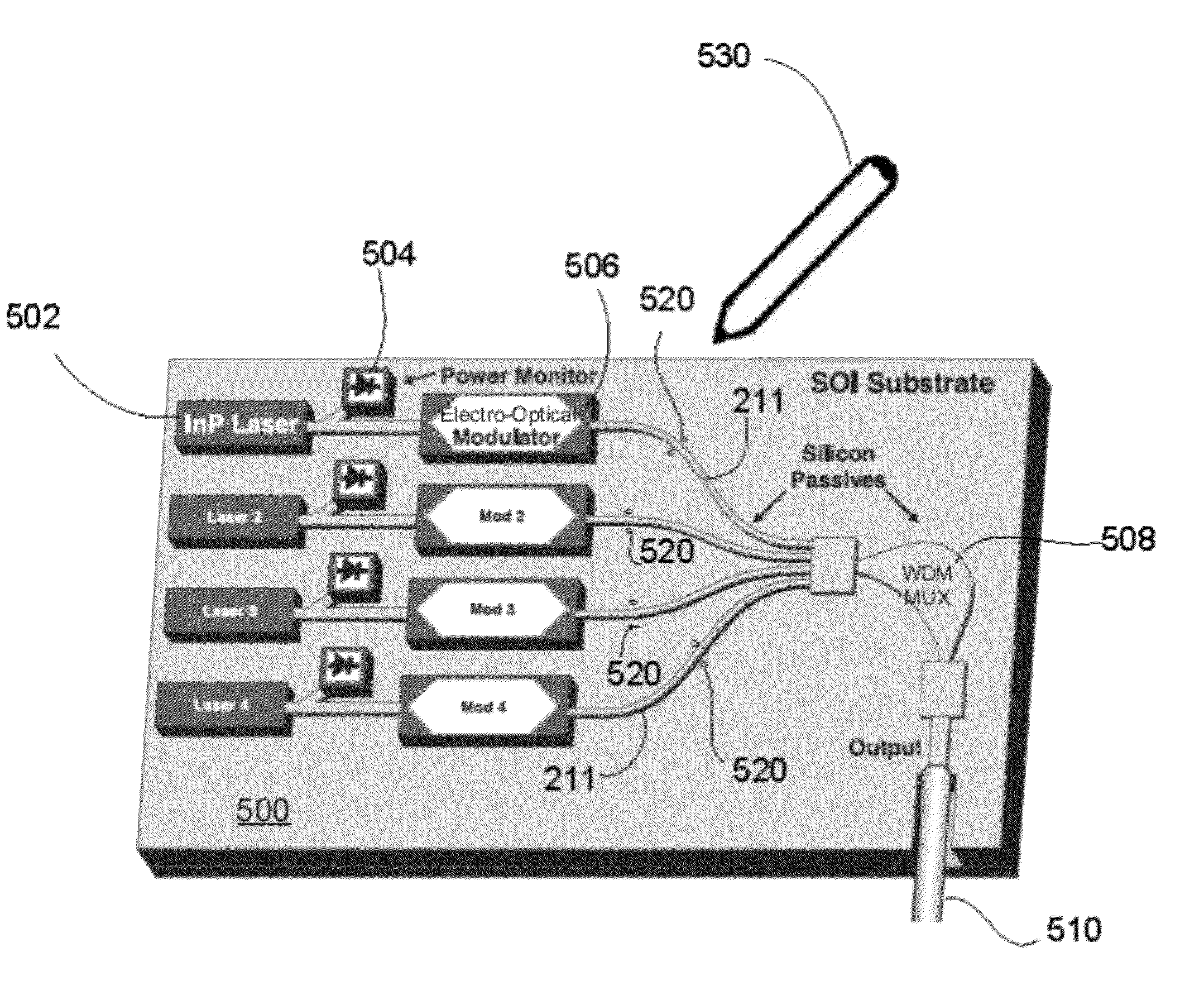
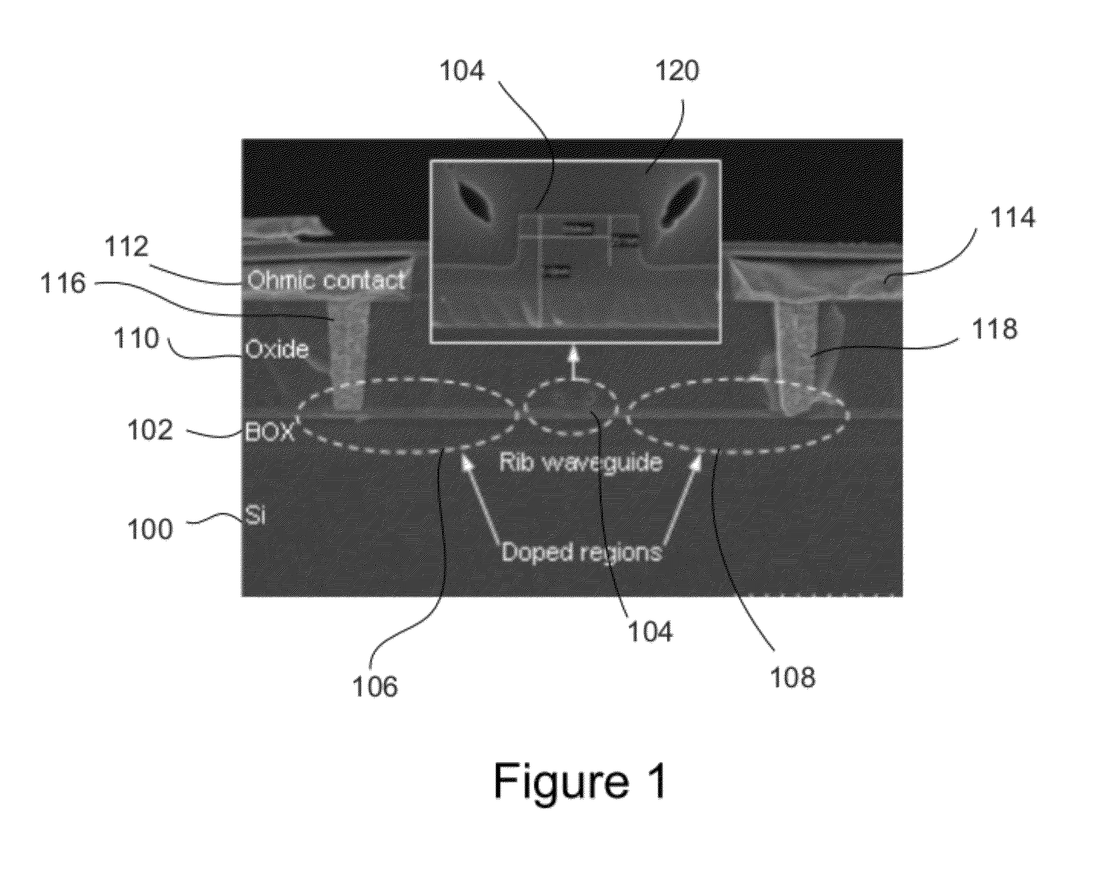
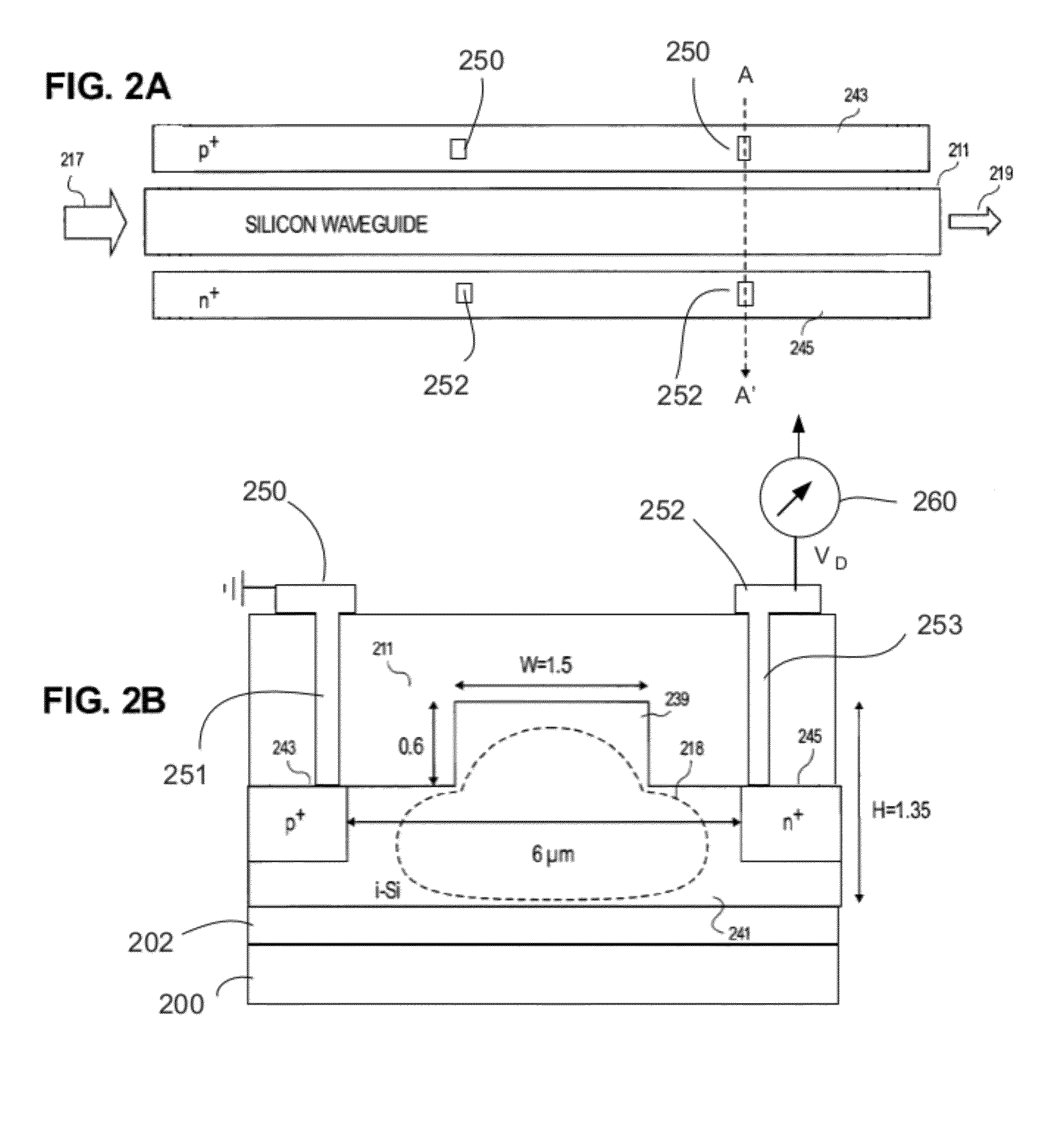
[0014]Described is a method and apparatus for in-situ optical power monitoring. In recent years silicon photonic components such as lasers, modulators, photo-detectors, wavelength converters, and wavelength multiplexers / demultiplexers have been developed. When integrating all these individual components onto a single silicon-based platform, it is desirable to be able to monitor the optical power of the integrated system at the chip-level. That is, the ability to monitor optical power at any desired point on chip is needed. Thus, in-situ power monitors would be useful in identifying and isolating the faulty component in a system without affecting the performance of a system.

[0015]Reference throughout this specification to “one embodiment” or “an embodiment” means that a particular feature, structure, or characteristic described in connection with the embodiment is included in at least one embodiment of the present invention. Thus, the appearances of the phrases “in one embodiment” or...


PUM


Abstract

Instead of monitoring the optical power coming out of a waveguide, a direct method of monitoring the optical power inside the waveguide without affecting device or system performance is provided. A waveguide comprises a p-i-n structure which induces a TPA-generated current and may be enhanced with reverse biasing the diode. The TPA current may be measured directly by probing metal contacts provided on the top surface of the waveguide, and may enable wafer-level testing. The p-i-n structures may be implemented at desired points throughout an integrated network, and thus allows probing of different devices for in-situ power monitor and failure analysis.

Description

FIELD OF THE INVENTION[0001]Embodiments of the present invention are directed to optical power monitoring and, more particularly, to in-situ optical power monitoring in a silicon waveguide.BACKGROUND INFORMATION[0002]High-bandwidth, power efficient, and reliable optical links have potential to change the consumer electronics and server markets as Internet data traffic continues to grow exponentially over the years and electronic interconnects are reaching their limits to sustain such growth. Integrated optoelectronic technology can serve as critical enabler to allow personal computing devices to send and receive data at unprecedented rate. In recent years, many successes in optical-component research in the field of silicon photonics have made silicon-on-insulator (SOI) the most promising material-platform-of-choice for the future generations of integrated optoelectronic systems. A typical integrated optoelectronic system could include lasers, modulators, multiplexers / demultiplexers...

Claims


Application Information

Patent Timeline
IPC IPC(8): H01L31/12H01L23/00H01L21/66
CPCH01L22/34H01L22/14H01L31/12G01J1/02
Inventor RONG, HAISHENGHSIEH, I-WEI ANDYPANICCIA, MARIO J.
Owner INTEL CORP
Why Eureka
Try Eureka