Collective printed circuit board

a printed circuit board and collective technology, applied in the direction of electrical apparatus casings/cabinets/drawers, electrical apparatus details, etc., can solve the problems of deterioration of operating efficiency, increased cost, and increased complexity of processes, so as to reduce the number of electronic devices, improve the effect of operating efficiency and high yield

Active Publication Date: 2012-04-05
KYOCERA CORP
View PDF0 Cites 58 Cited by
  • Summary
  • Abstract
  • Description
  • Claims
  • Application Information

AI Technical Summary

Benefits of technology

[0011]According to the present invention, since one collective printed circuit board is formed by independently bonding a plurality of printed circuit boards to a frame, only non-defective printed circuit boards can be selected and bonded to the frame. In this manner, a collective printed circuit board in which printed circuit boards having a very high yield are arranged can be formed. Thus, the number of electronic devices that can be simultaneously manufactured from one collective printed circuit board can be prevented from decreasing, and the problem such as deterioration of operating efficiency or an increase in cost can be solved.
[0012]According to the present invention, the rigidity can be improved by the frame, the upper-surface peripheral edge portions of the printed circuit boards are bonded to lower surfaces of the peripheral portions of the through holes formed in the frame such that semiconductor element mounting units are exposed from the through holes. For this reason, an amount of sealing resin can be minimized to suppress the upper-surface sides of the printed circuit boards from being deformed into a concave shape. In this manner, there can be provided a collective printed circuit board in which semiconductor elements are mounted on flat printed circuit boards and that can stably supply electronic devices that can be preferably mounted on another circuit board.

Problems solved by technology

However, in recent years, with advances in miniaturization and multi-layering of circuits of collective printed circuit boards, processes become complicated and difficult, a yield of printed circuit boards in a collective printed circuit board tends to decrease.
For this reason, the number of electronic devices that can be simultaneously manufactured from one collective printed circuit board decreases, a problem such as deterioration of operating efficiency and an increase in cost is posed.
As a result, the printed circuit board is warped such that an upper surface side of the printed circuit board is concaved.
When the warpage is large, electronic devices formed by cutting the collective printed circuit board are difficult to be mounted on another circuit board.

Method used


Image

  • Collective printed circuit board
  • Collective printed circuit board
  • Collective printed circuit board

Examples


Embodiment Construction

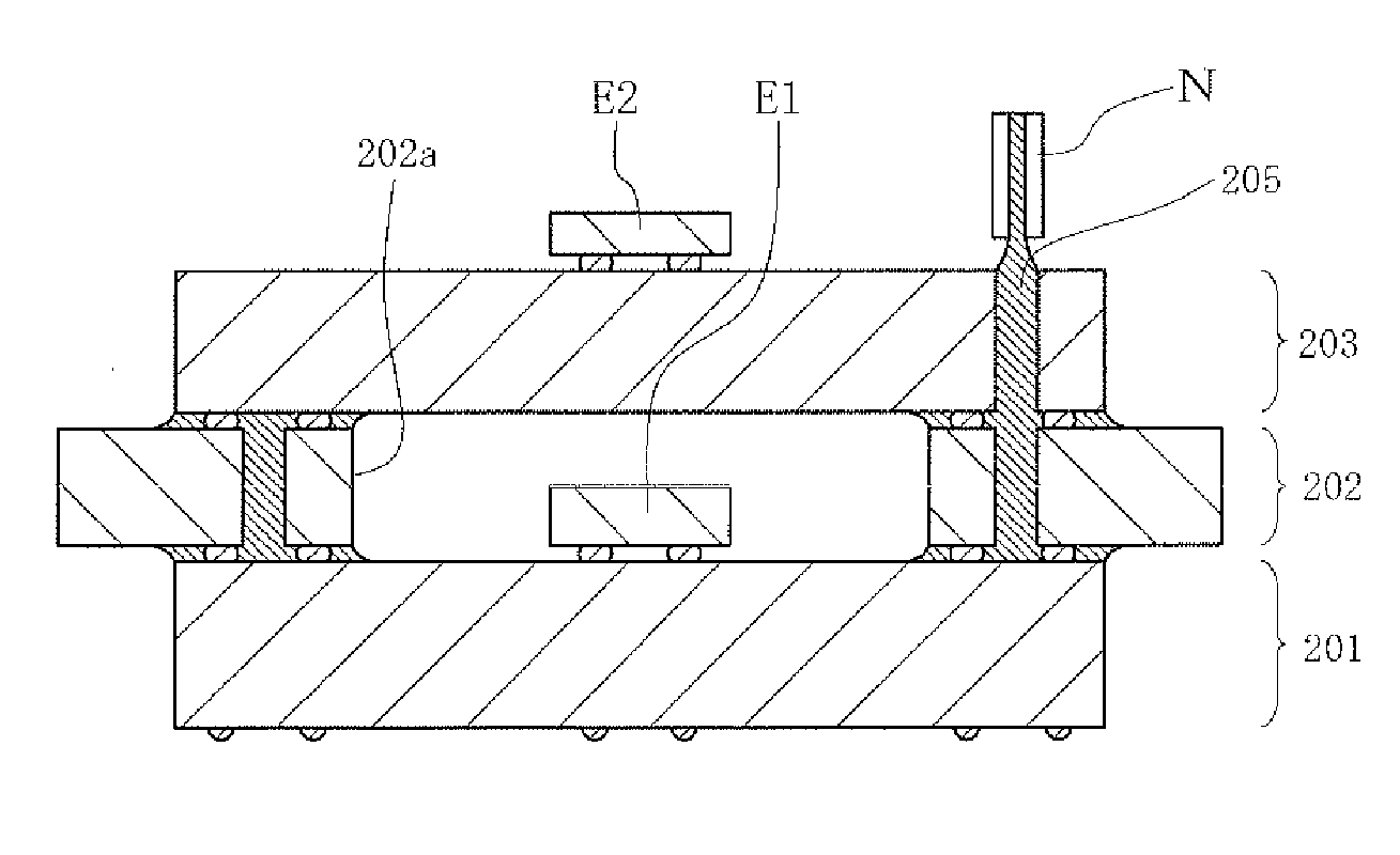
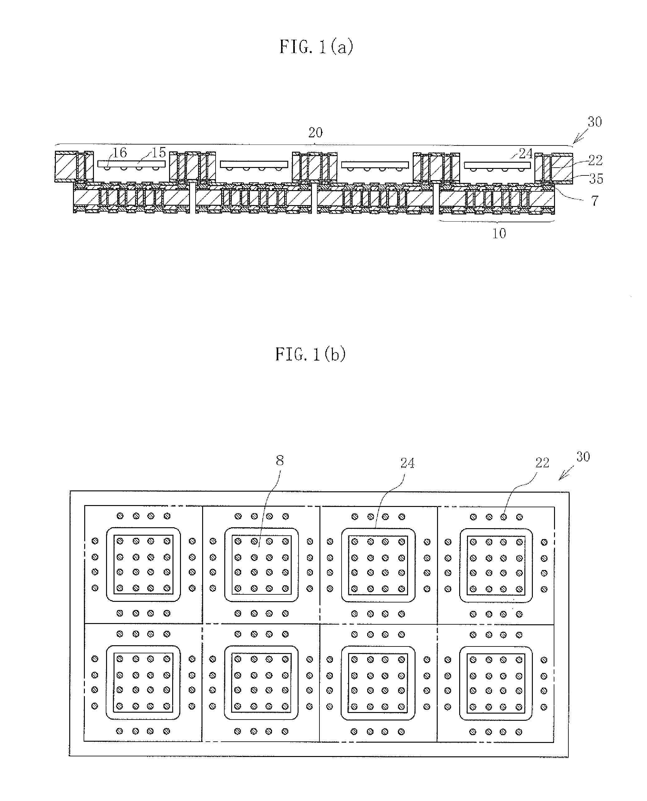
[0027]An example of an embodiment of a collective printed circuit board according to the present invention will be described below with reference to FIGS. 1 to 9. As shown in these drawings, a collective printed circuit board 30 of this example is mainly configured by a printed circuit board 10 and a frame 20.

[0028]As shown in FIG. 1, a plurality of small printed circuit board 10 to mount a semiconductor element 15 thereon are bonded to a lower surface of the frame 20 to support the printed circuit boards 10.

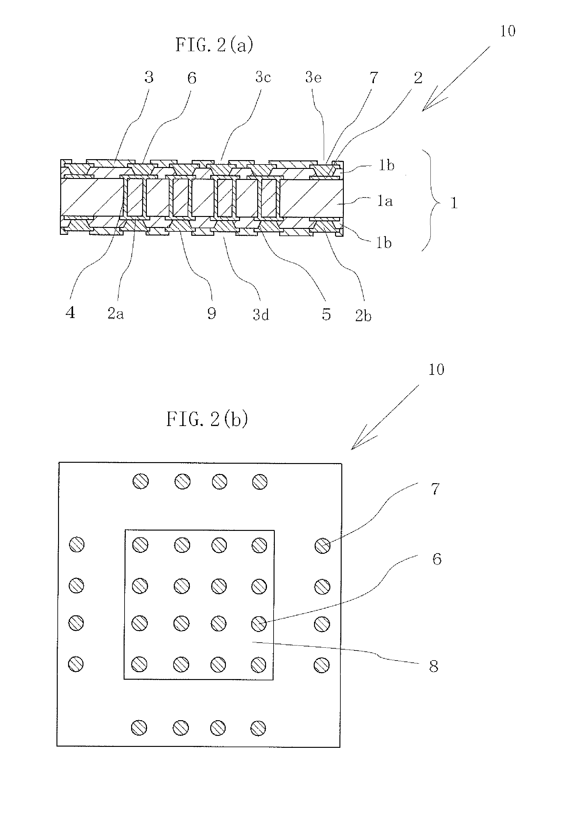
[0029]Each of the printed circuit boards 10 includes, as shown in FIGS. 2A and 2B, for example, an insulating substrate 1 obtained by stacking insulating layers 1b on upper and lower sides of an insulating plate 1a, respectively, conductive layers 2 formed on the insulating plate 1a and the insulating layer 1b, and a solder resist layer 3 used as a protective layer. A mounting portion 8 on which the semiconductor element 15 is mounted is formed on an upper-surface central portio...


PUM


Abstract

There is provided a collective printed circuit board including a plurality of printed circuit boards each having a mounting unit on which a semiconductor element is mounted at an upper-surface central portion, and a frame having a plurality of through holes having sizes to surround the mounting portion. Upper-surface peripheral edge portions of the printed circuit boards and a through-hole peripheral portion of the frame are bonded to each other such that the mounting units are exposed from the through holes.

Description

BACKGROUND OF THE INVENTION[0001](1) Field of the Invention[0002]The present invention relates to a collective printed circuit board obtained by bonding a plurality of small printed circuit boards each having a mounting unit on which a semiconductor element is mounted to a frame having through holes surrounding the mounting units.[0003](2) Description of Related Art[0004]Conventionally, in order to simultaneously manufacture a large number of small printed circuit boards to mount semiconductor elements thereon as disclosed in Unexamined Patent Publication No. 1998-189829, Unexamined Patent Publication No. 2001-210954, and Published Japanese Translation No. 2001-511946 of the PCT International Publication (U.S. Pat. No. 6,329,606), a collective printed circuit board is used. In the collective printed circuit board, a plurality of small printed circuit boards are integrally arranged in vertical and horizontal directions such that cutting areas are formed between the small printed circ...

Claims


Application Information

Patent Timeline
Patent Type & Authority Applications(United States)
IPC IPC(8): H05K7/14
CPCH01L23/49816H01L23/49822H01L2924/15311H01L2224/73204H01L2224/32225H01L2224/16225H01L2225/107H01L2924/3511H01L2224/73253H05K2201/2018H01L23/49827H01L23/49833H01L23/5389H01L25/0652H01L25/0655H01L25/105H01L25/16H01L2225/1023H01L2225/1058H05K3/0052H05K3/0097H05K3/284H05K2201/042H05K2201/10674H01L2924/00012H01L2924/00H01L2224/32014H05K1/144
Inventor SAKURAI, KEIZOUTAKAGI, TOSHIAKI
Owner KYOCERA CORP
Why Eureka
Try Eureka