Low voltage programming in NAND flash

a low-voltage programming and nand flash technology, applied in static storage, digital storage, instruments, etc., can solve the problems of limiting the ability to increase the density of flash memory, introducing complexity in manufacturing processes, and interfering between the charge stored in adjacent floating gates becomes a problem

Active Publication Date: 2012-04-05
MACRONIX INT CO LTD
View PDF6 Cites 43 Cited by
  • Summary
  • Abstract
  • Description
  • Claims
  • Application Information

AI Technical Summary

Benefits of technology

[0013]In a second plurality of memory cells coupled to the same plurality of word lines, such as a parallel NAND string on an unselected bit line, the control circuitry can operate to apply a common voltage (e.g., a source side voltage or a drain side voltage) to both the first and second ends of the plurality of transistors. In this arrangement, the semiconductor body regions on both sides of the selected word line are biased to similar voltage levels to prevent hot carrier injection in unselected strings.

Problems solved by technology

As the density increases in memory devices, and the floating gate memory cells get closer and closer together, interference between the charge stored in adjacent floating gates becomes a problem.
This is limiting the ability to increase the density of flash memory based on floating gate memory cells.
The addition of high voltage transistors on integrated circuits, in combination with transistors used for logic and other data flow, introduces complexity in the manufacturing processes.
This increased complexity in turn increases the costs of the devices.

Method used


Image

  • Low voltage programming in NAND flash
  • Low voltage programming in NAND flash
  • Low voltage programming in NAND flash

Examples


Embodiment Construction

[0038]A detailed description of embodiments of the present invention is provided with reference to the FIGS. 1-22.

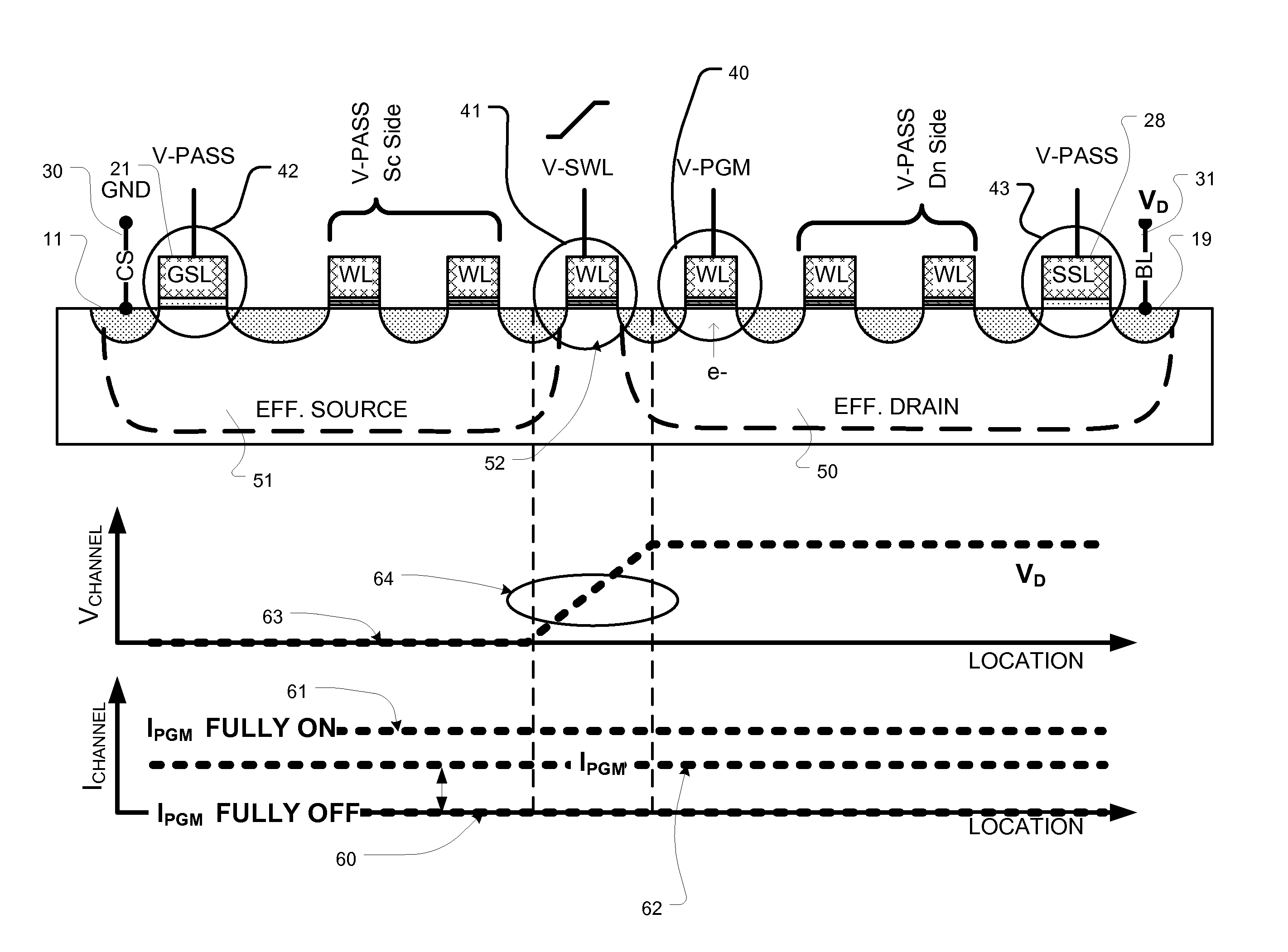
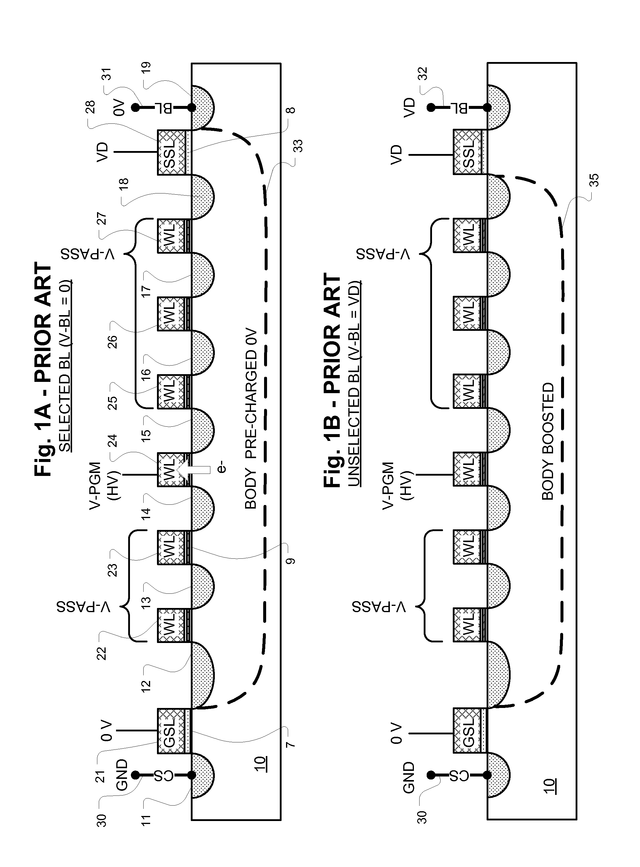
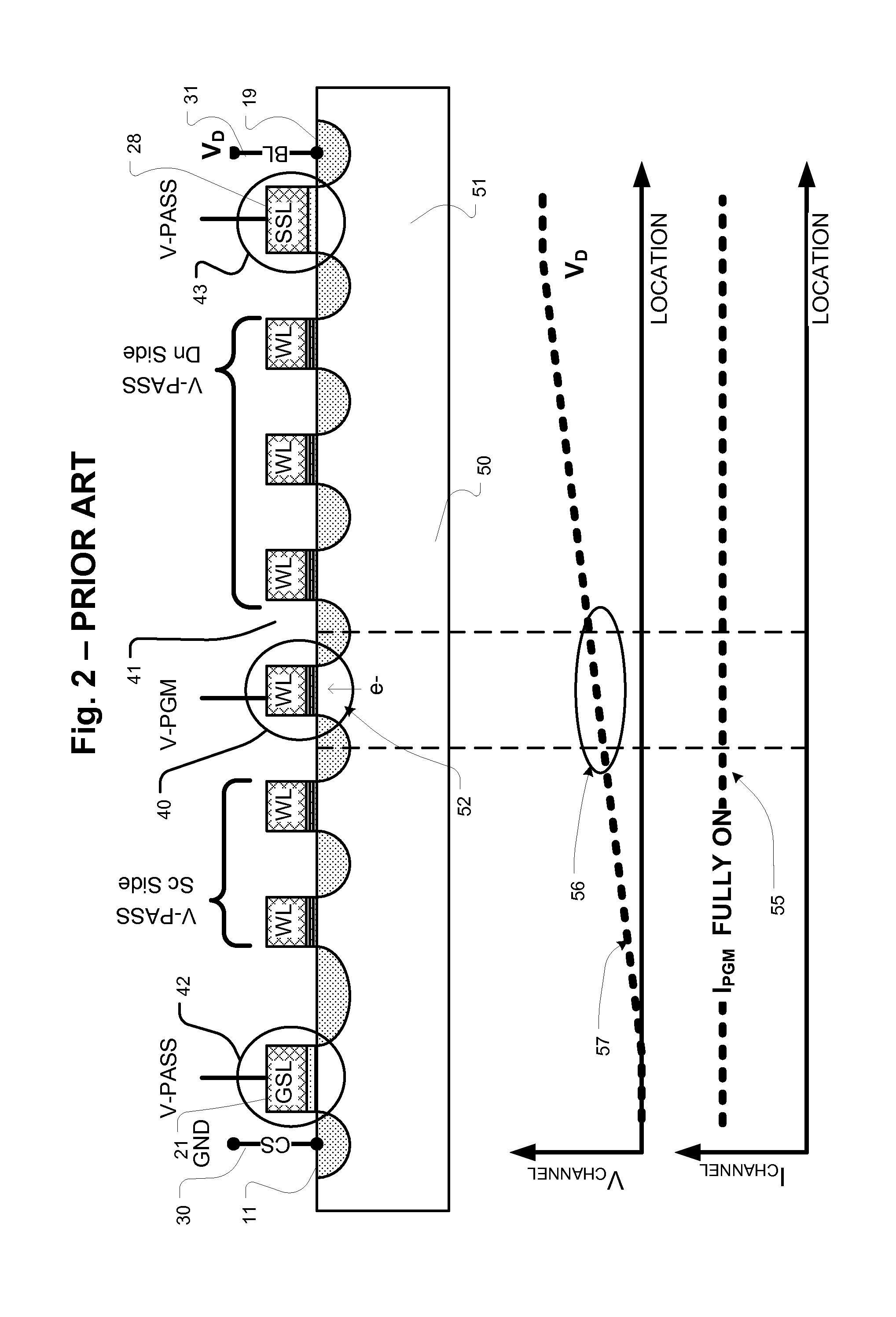
[0039]FIGS. 1A and 1B show in cross-section a plurality of dielectric charge trapping flash memory cells arranged in series to form a NAND string and biased for FN tunneling programming, as is typical in prior art NAND architecture flash memory. FIG. 1A shows the biasing for a NAND string that includes a target cell on a selected bit line, while FIG. 1B shows the biasing for a NAND string on an unselected bit line. One technology for implementation of NAND flash using bandgap engineered SONOS (BE-SONOS) charge trapping technology is described in U.S. Pat. No. 7,315,474 by Lue, which is incorporated by reference as if fully set forth herein. NAND strings can be implemented in a variety of configurations, including finFET technology, shallow trench isolation technology, vertical NAND technology and others. See, for an example vertical NAND structures, European Patent Appli...


PUM


Abstract

A memory device includes a plurality of memory cells arranged in series in the semiconductor body, such as a NAND string, having a plurality of word lines. A selected memory cell is programmed by hot carrier injection. The program operation is based on metering a flow of carriers between a first semiconductor body region on a first side of the selected cell in the NAND string and a second semiconductor body region on a second side of the selected cell. A program potential higher than a hot carrier injection barrier level is applied to the selected cell, and then the drain to source voltage across the selected cell and the flow of carriers in the selected cell reach a level sufficient to support hot carrier injection, which is controlled by a switch cell adjacent the selected cell.

Description

REFERENCE TO RELATED APPLICATION[0001]This application claims the benefit under 35 U.S.C. §119(e) of U.S. Provisional Application No. 61 / 388,505, filed on 30 Sep. 2010, which is incorporated herein by reference.[0002]The present application is related to co-pending U.S. patent application Ser. No. 12 / 797,994, entitled HOT CARRIER PROGRAMMING IN NAND FLASH, filed on 10 Jun. 2010, invented by Jyun-Siang HUANG and Wen-Jer TSAI (MXIC1935-1), and is owned by a common assignee.BACKGROUND OF THE INVENTION[0003]1. Field of the Invention[0004]The present invention relates to flash memory technology, and more particularly to flash memory suitable for low voltage program and erase in a NAND configuration.[0005]2. Description of Related Art[0006]Flash memory is a class of non-volatile integrated circuit memory technology. Traditional flash memory employs floating gate memory cells. As the density increases in memory devices, and the floating gate memory cells get closer and closer together, int...

Claims


Application Information

Patent Timeline
Patent Type & Authority Applications(United States)
IPC IPC(8): G11C16/04
CPCG11C16/0483G11C16/3427G11C16/10
Inventor TSAI, PING-HUNGHUANG, JYUN-SIANGTSAI, WEN-JER
Owner MACRONIX INT CO LTD
Why Eureka
Try Eureka