Detecting circuit for pixel electrode voltage of flat panel display device
- Summary
- Abstract
- Description
- Claims
- Application Information
AI Technical Summary
Benefits of technology
Problems solved by technology
Method used
Image
Examples
first embodiment
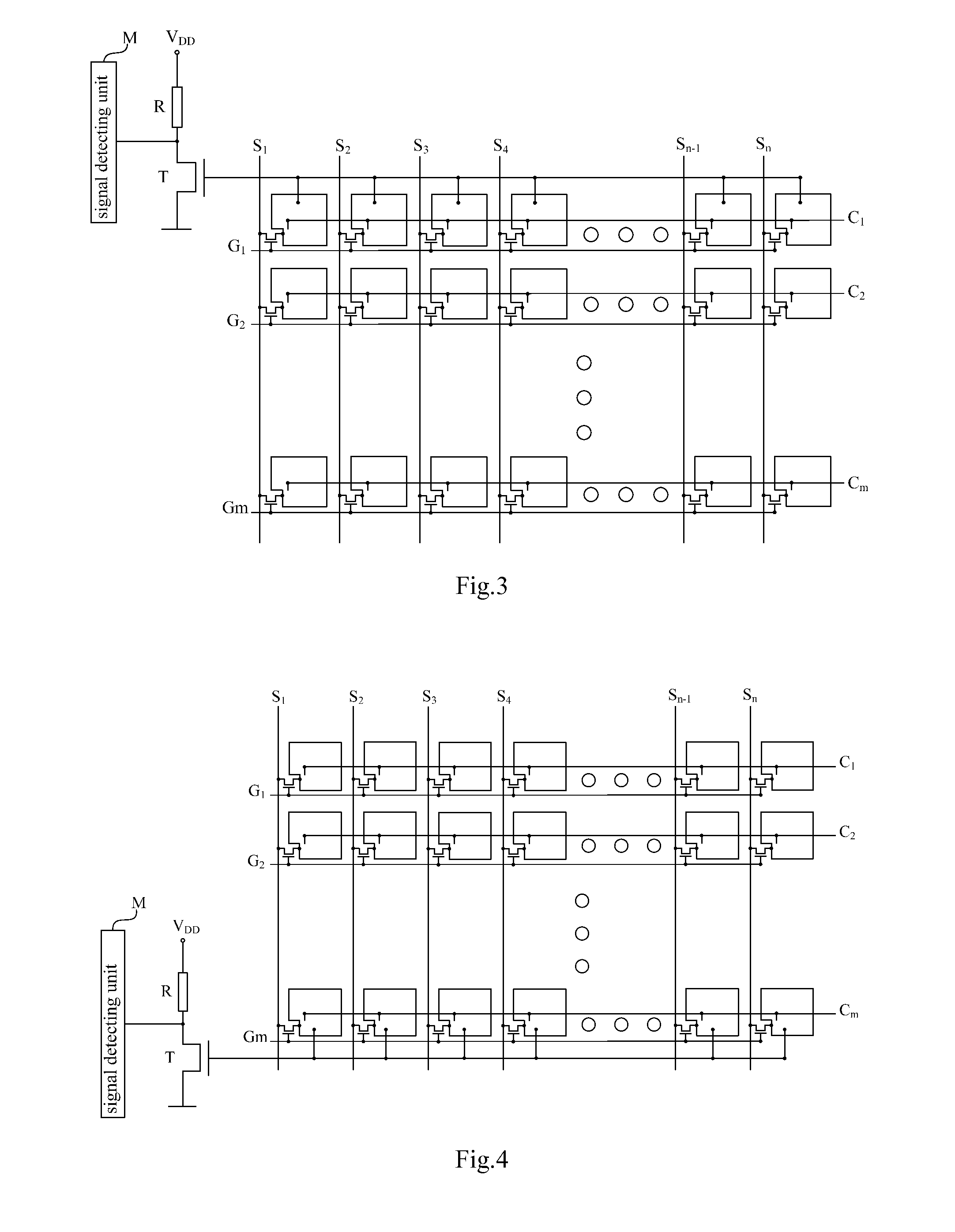
[0042]FIG. 3 shows a schematic circuit structure diagram of a detecting circuit for pixel electrode voltage according to the present invention used in a thin film transistor liquid crystal display device. FIG. 3 is an illustrative explanation, and only a part of the thin film transistor liquid crystal display device is shown; furthermore, the structure of the liquid crystal display device is simplified and partly omitted herein, and only the components that are related to the embodiments of the present invention are shown, which is not intended to limit the scope of protection thereto. As shown in FIG. 3, the liquid crystal display device includes an active matrix region, and the active matrix region includes: pixel units including thin film transistors (TFTs) serving as switching elements and pixel electrodes connected with drains of the TFTs; a plurality of scanning lines G1, G2, . . . , Gm (m is a natural number) extending in a horizontal direction and connected to gates of the T...
second embodiment
[0051]FIG. 5 shows a schematic structural diagram of a detecting circuit for pixel electrode voltage according to the present invention used in a thin film transistor liquid crystal display device.
[0052]In the second embodiment, the components same as or similar to those in the first embodiment are indicated by same or similar component numerals, and a detailed explanation thereof is omitted herein, to make the description of the present invention be clear and intelligible.
[0053]The major difference of the second embodiment from the first embodiment lies in the connection between the pixel electrode of the pixel unit and the MOS transistor T serving as the signal amplifying unit. In the second embodiment, the pixel electrodes of the pixel units located in the odd columns of the first row are connected with the gate of the MOS transistor T.
[0054]In the detecting circuit for pixel electrode voltage according to the second embodiment, the approach of connecting the pixel electrodes of ...
third embodiment
[0055]FIG. 7 shows a schematic structural diagram of a detecting circuit for pixel electrode voltage according to the present invention used in a thin film transistor liquid crystal display device.
[0056]In the third embodiment, the components same as or similar to those in the first embodiment are indicated by same or similar component numerals, and a detailed explanation thereof is omitted herein, to make the description of the present invention be clear and intelligible.
[0057]The major difference of the third embodiment from the first embodiment lies in that the detecting sub-circuit for pixel electrode voltage further includes a MOS transistor T2 serving as a preset unit. The MOS transistor T2 is located between the MOS transistor T1 serving as the signal amplifying unit and the pixel electrode of the pixel unit connected with the MOS transistor T1, and the drain of the MOS transistor T2 is connected with the gate of the MOS transistor T1, in order to preset the characteristics o...
PUM
 Abstract
Description
Claims
Application Information


