Detecting circuit for pixel electrode voltage of flat panel display device

a flat panel display and detection circuit technology, applied in the direction of electrical testing, measurement devices, instruments, etc., can solve the problems of inability to acquire the exact capacitance value in the practical application, inconvenient individual processing to compensate the aging and drift of the product, and inability to adjust the common electrode voltage vcom to compensate the voltage. , to achieve the effect of simple detection circuit and accurate detection results

Active Publication Date: 2015-05-26
BEIHAI HKC OPTOELECTRONICS TECH CO LTD
View PDF27 Cites 0 Cited by
  • Summary
  • Abstract
  • Description
  • Claims
  • Application Information

AI Technical Summary

Benefits of technology

[0013]The problem solved by the present invention is to provide a detecting circuit for pixel electrode voltage of a flat panel display device, to avoid the problems in the prior art of complex structure of the detecting circuit for pixel electrode voltage, or lower accuracy in detecting the pixel electrode voltage caused by the influence of its electronic characteristics on the pixel electrode, and so on.
[0028]The present invention provides a detecting circuit for pixel electrode voltage of a flat panel display device, in which a voltage signal of the pixel electrode can be amplified by the signal amplifying unit therein, so it is convenient to observe the voltage signal of the pixel electrode, then to detect the voltage signal variation of the pixel electrode with time. Compared with the prior art, the present invention has advantages of a simple detecting circuit and an accurate detection result.

Problems solved by technology

And in other cases, because the variations of the kickback voltages in different liquid crystal pixel electrodes are not the same, the approach of adjusting the common electrode voltage Vcom can not be adopted to compensate the voltage.
However, the method mentioned above has the problems of design constraints and complex fabrication process, and it is difficult to acquire an exact capacitance value in the practical application.
However, this compensational adjustment has the following drawbacks: being complex in operation, and being time-consuming and energy-consuming; because the voltage variation of the pixel electrode is estimated indirectly from experience and the computer simulation, it can not be assured to obtain the exact voltage variation of the pixel electrode, which may affect the subsequent compensation result; and it is inconvenient to perform individual processing to compensate the aging and the drift of the product during usage in time for each product in the practical application.
Moreover, if the pixel electrode voltage is inducted by an external induction circuit (such as an amplifier or an oscilloscope etc.), because the capacitance value of the induction circuit itself may apparently affect the liquid crystal pixel unit having a small capacitance value (0.1 pF to 1 pF), the variation of the pixel voltage can not be detected accurately as well.

Method used


Image

  • Detecting circuit for pixel electrode voltage of flat panel display device
  • Detecting circuit for pixel electrode voltage of flat panel display device
  • Detecting circuit for pixel electrode voltage of flat panel display device

Examples


first embodiment

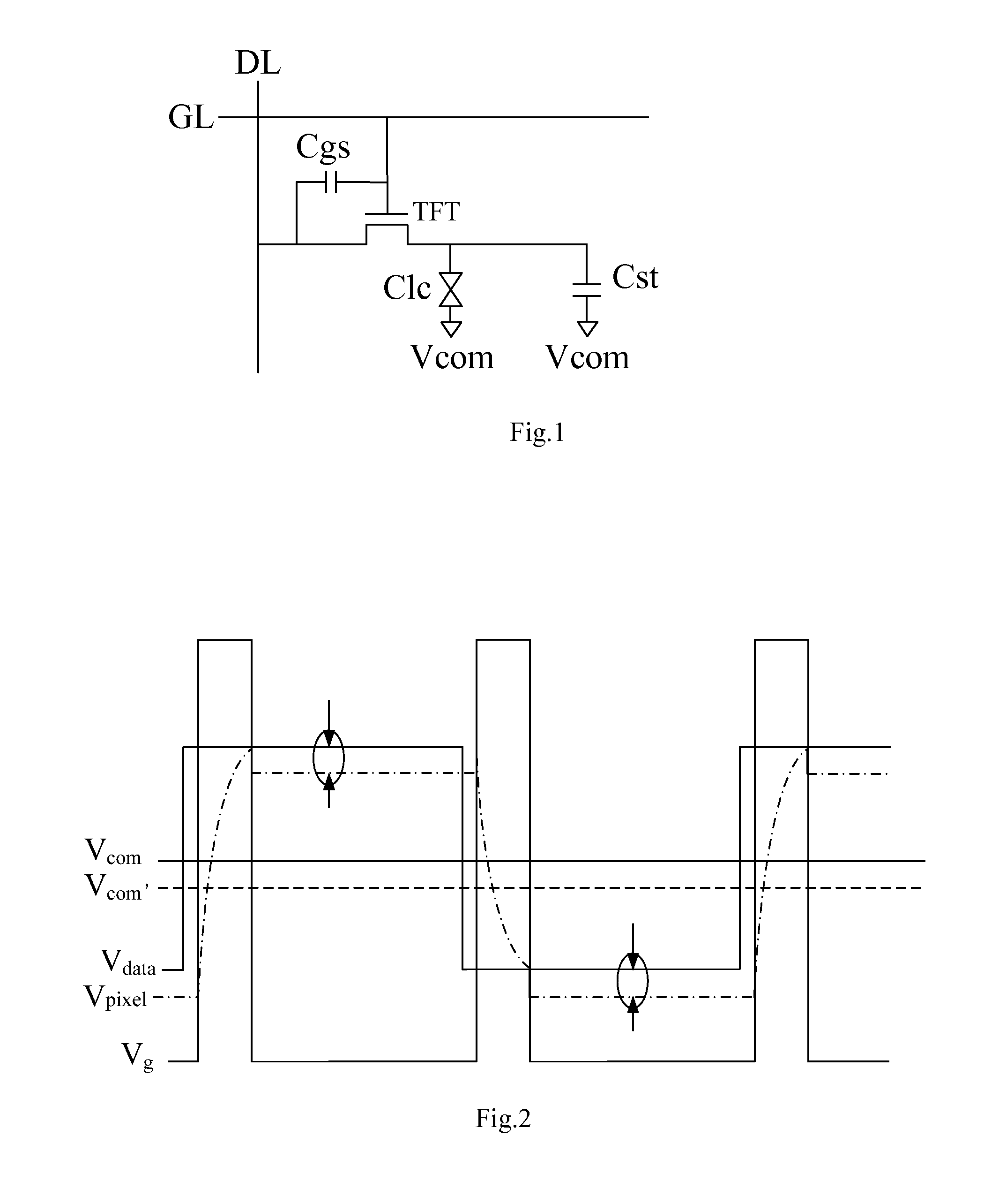
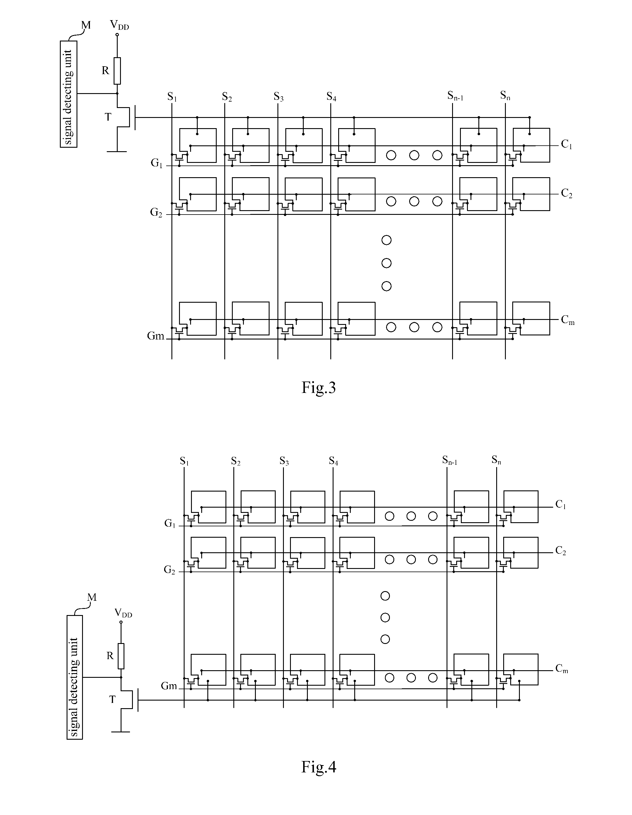
[0042]FIG. 3 shows a schematic circuit structure diagram of a detecting circuit for pixel electrode voltage according to the present invention used in a thin film transistor liquid crystal display device. FIG. 3 is an illustrative explanation, and only a part of the thin film transistor liquid crystal display device is shown; furthermore, the structure of the liquid crystal display device is simplified and partly omitted herein, and only the components that are related to the embodiments of the present invention are shown, which is not intended to limit the scope of protection thereto. As shown in FIG. 3, the liquid crystal display device includes an active matrix region, and the active matrix region includes: pixel units including thin film transistors (TFTs) serving as switching elements and pixel electrodes connected with drains of the TFTs; a plurality of scanning lines G1, G2, . . . , Gm (m is a natural number) extending in a horizontal direction and connected to gates of the T...

second embodiment

[0051]FIG. 5 shows a schematic structural diagram of a detecting circuit for pixel electrode voltage according to the present invention used in a thin film transistor liquid crystal display device.

[0052]In the second embodiment, the components same as or similar to those in the first embodiment are indicated by same or similar component numerals, and a detailed explanation thereof is omitted herein, to make the description of the present invention be clear and intelligible.

[0053]The major difference of the second embodiment from the first embodiment lies in the connection between the pixel electrode of the pixel unit and the MOS transistor T serving as the signal amplifying unit. In the second embodiment, the pixel electrodes of the pixel units located in the odd columns of the first row are connected with the gate of the MOS transistor T.

[0054]In the detecting circuit for pixel electrode voltage according to the second embodiment, the approach of connecting the pixel electrodes of ...

third embodiment

[0055]FIG. 7 shows a schematic structural diagram of a detecting circuit for pixel electrode voltage according to the present invention used in a thin film transistor liquid crystal display device.

[0056]In the third embodiment, the components same as or similar to those in the first embodiment are indicated by same or similar component numerals, and a detailed explanation thereof is omitted herein, to make the description of the present invention be clear and intelligible.

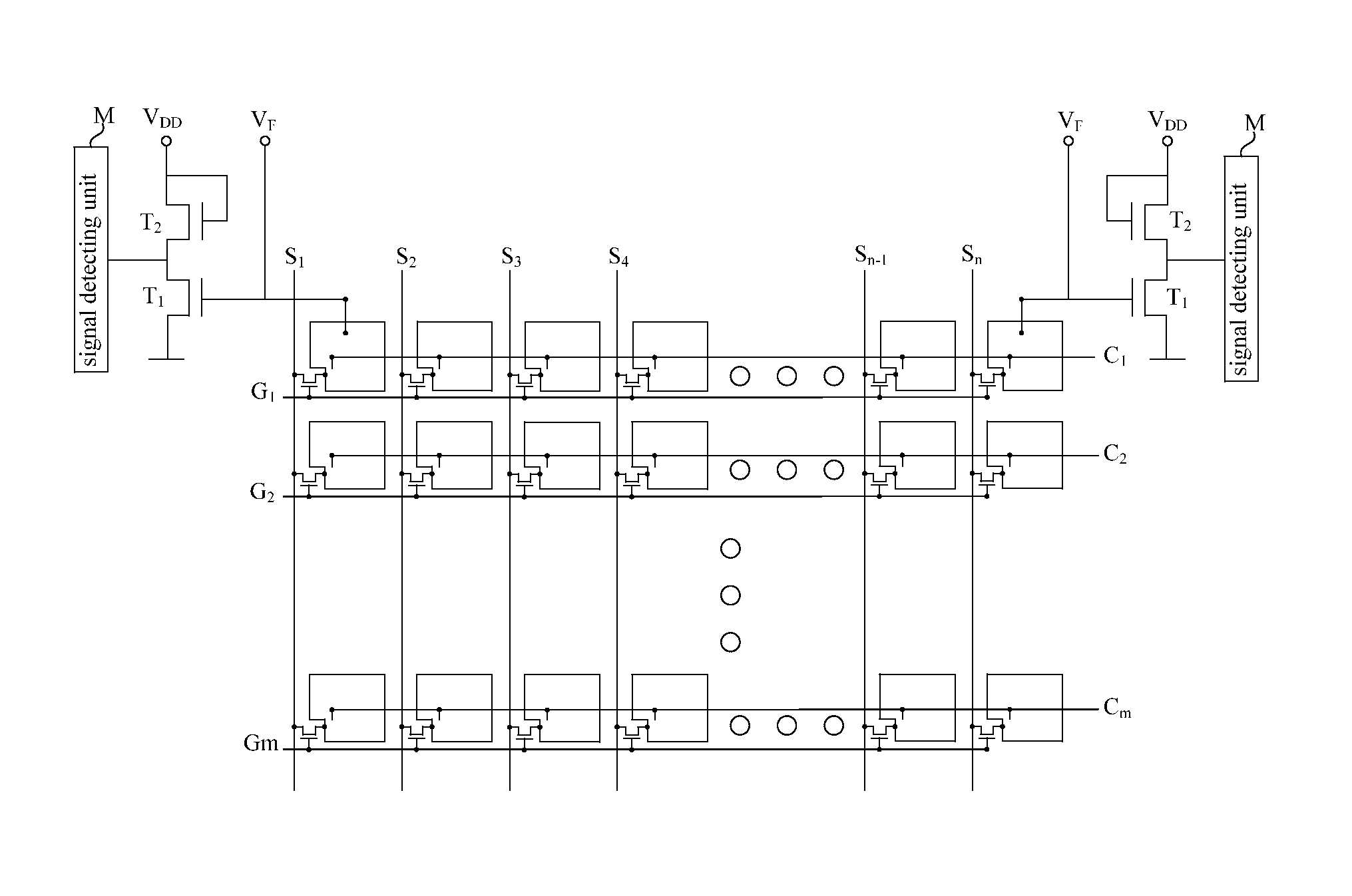
[0057]The major difference of the third embodiment from the first embodiment lies in that the detecting sub-circuit for pixel electrode voltage further includes a MOS transistor T2 serving as a preset unit. The MOS transistor T2 is located between the MOS transistor T1 serving as the signal amplifying unit and the pixel electrode of the pixel unit connected with the MOS transistor T1, and the drain of the MOS transistor T2 is connected with the gate of the MOS transistor T1, in order to preset the characteristics o...


PUM

PropertyMeasurementUnit
capacitanceaaaaaaaaaa
voltageaaaaaaaaaa
polaritiesaaaaaaaaaa

Abstract

A detecting circuit for pixel electrode voltage of a flat panel display device, the flat panel display device having a plurality of scanning lines and a plurality of data lines crossing with the plurality of scanning lines, the plurality of scanning lines and data lines define a plurality of pixel units, and each of the pixel units including a pixel switching element and a pixel electrode. The detecting circuit for pixel electrode voltage includes at least one detecting sub-circuit for pixel electrode voltage. The detecting sub-circuit for pixel electrode voltage includes: a signal amplifying unit connected with the pixel electrode in the pixel unit, for amplifying a voltage signal of the pixel electrode; and a signal detecting unit connected with the signal amplifying unit, for detecting the voltage signal of the pixel electrode that has been amplified by the signal amplifying unit, and outputting a variation in the voltage signal of the pixel electrode with time. Compared with the prior art, the present invention has advantages of simple detecting circuit structure and accurate detection result.

Description

CROSS REFERENCE TO RELATED APPLICATION[0001]This application claims the benefit of priority to Chinese Patent Application No. 201010509158.3, entitled “Detecting Circuit for Pixel Electrode Voltage of Flat Panel Display Device”, filed on Oct. 14, 2010 with State Intellectual Property Office of PRC, which is incorporated herein by reference in its entirety.BACKGROUND OF THE INVENTION[0002]1. Field of the Invention[0003]The present invention relates to flat panel display technique, and particularly to a detecting circuit for pixel electrode voltage of a flat panel display.[0004]2. Related Art[0005]Liquid crystal display (LCD) devices have been widely used in various data processing equipments such as TV, notebook computer, mobile telephone, personal digital assistant, etc., due to the advantages of lighter weight, thinner thickness, smaller footprint, lower power consumption, lower radiation, and so on. With the continuous development of the electronic industry, the performance of the...

Claims


Application Information

Patent Timeline
Patent Type & Authority Patents(United States)
IPC IPC(8): G01R31/26G02F1/13G09G3/36
CPCG09G3/3648G09G3/3655G02F1/1309G09G2320/0209G09G3/3614G09G2320/0223
Inventor HUANG, ZHONGSHOU
Owner BEIHAI HKC OPTOELECTRONICS TECH CO LTD
Why Eureka
Try Eureka