Method for Integrated Circuit Manufacturing and Mask Data Preparation Using Curvilinear Patterns

a curvilinear pattern and integrated circuit technology, applied in the field of manufacturing integrated circuits, can solve the problems of affecting the functional or parametric yield of an integrated circuit, affecting the accuracy of the physical design to the actual circuit pattern developed on the resist layer, and relatively large changes in curvilinear pattern on the substra

Active Publication Date: 2012-04-19
D2S
View PDF2 Cites 23 Cited by
  • Summary
  • Abstract
  • Description
  • Claims
  • Application Information

AI Technical Summary

Problems solved by technology

An example of an end-use limitation is defining the geometry of a transistor in a way in which it cannot sufficiently operate at the required supply voltage.
The design rule limitations reflect, among other things, the smallest dimensions that can be reliably fabricated.
As the critical dimensions of the circuit pattern become smaller and approach the resolution value of the exposure tool, the accurate transcription of the physical design to the actual circuit pattern developed on the resist layer becomes difficult.
However, because of

Method used


Image

  • Method for Integrated Circuit Manufacturing and Mask Data Preparation Using Curvilinear Patterns
  • Method for Integrated Circuit Manufacturing and Mask Data Preparation Using Curvilinear Patterns
  • Method for Integrated Circuit Manufacturing and Mask Data Preparation Using Curvilinear Patterns

Examples


Embodiment Construction

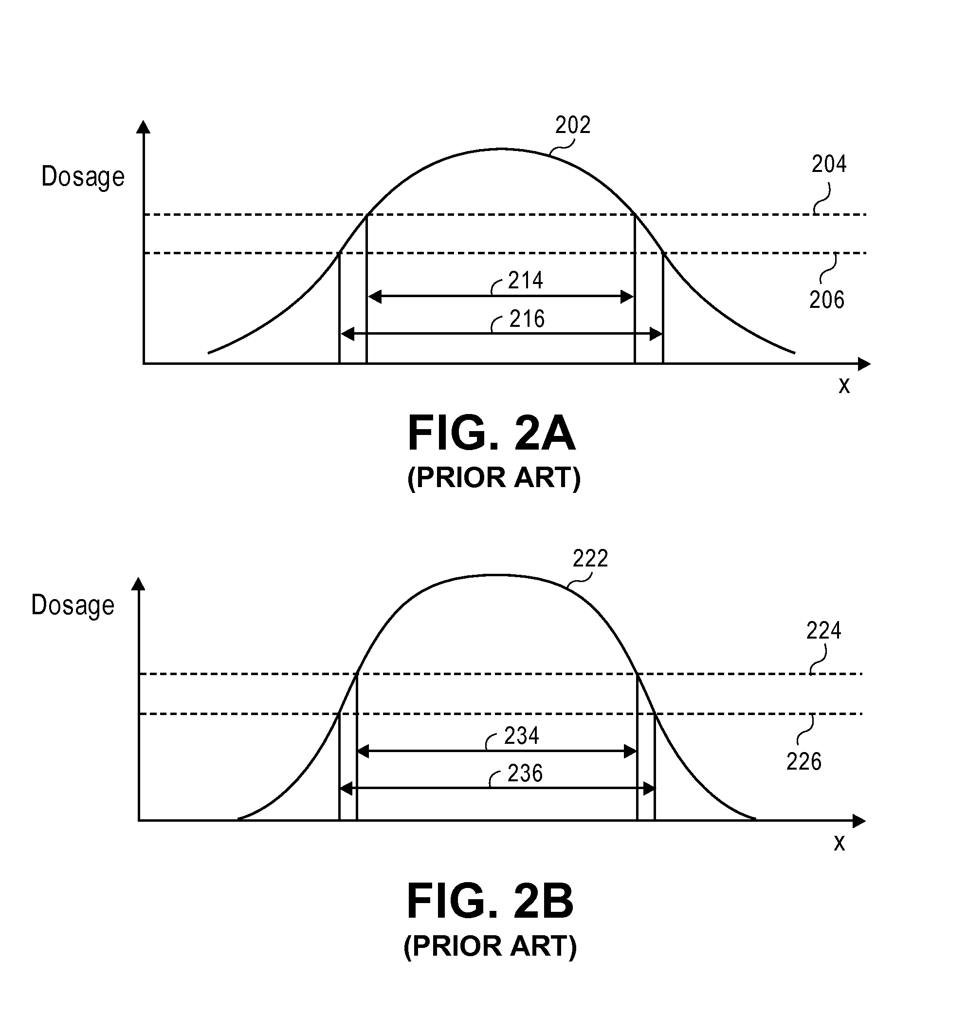
[0042]The current invention utilizes curvilinear patterns on the mask to produce curvilinear patterns on the substrate. The use of a curvilinear pattern on the mask which more closely matches the expected curvilinear pattern on the substrate reduces the sensitivity of the substrate pattern to process variations. In some embodiments, curvilinear patterns are designed into the layout in the design phase. In other embodiments, manhattan patterns in the originally-designed layout are later modified into curvilinear patterns.

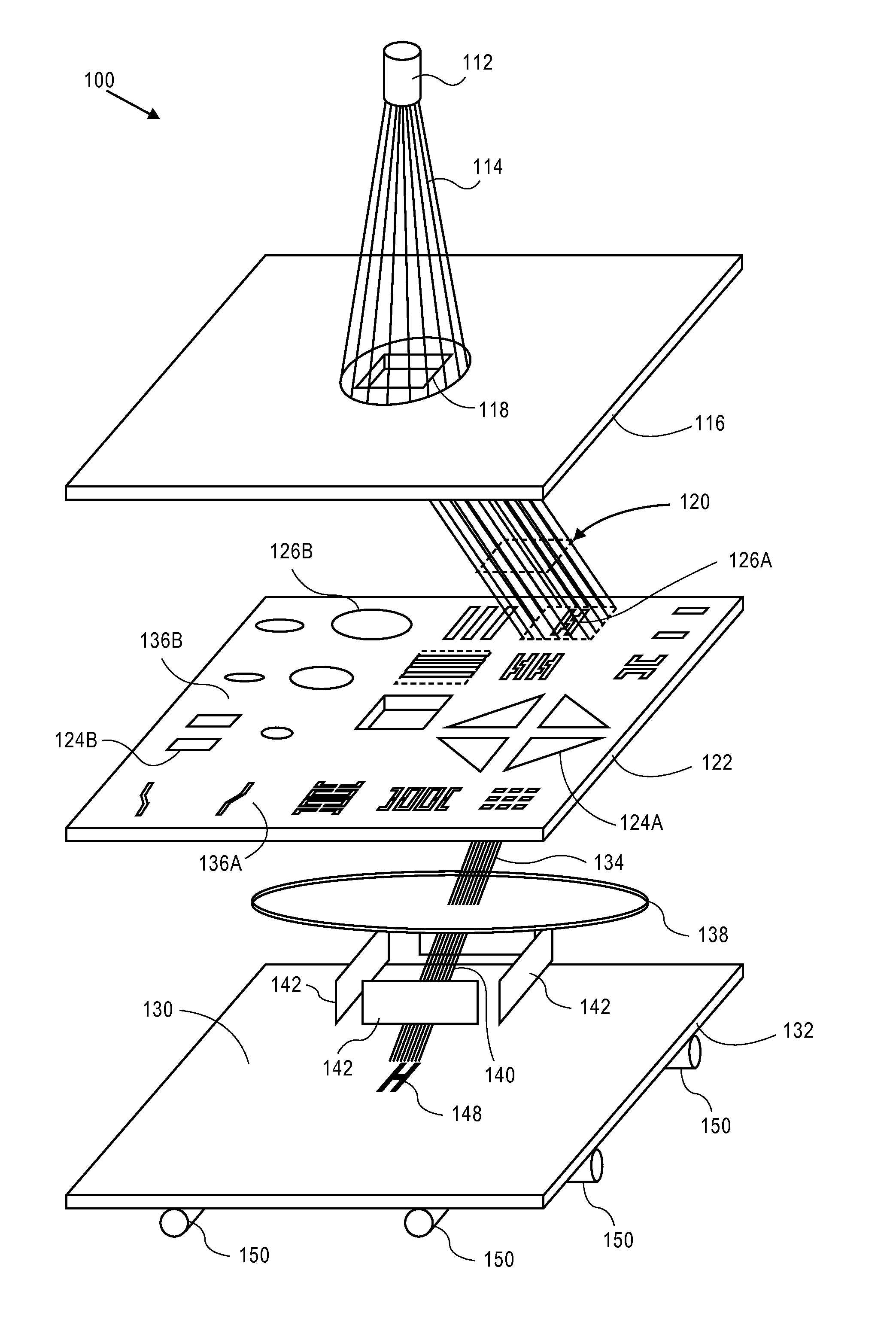
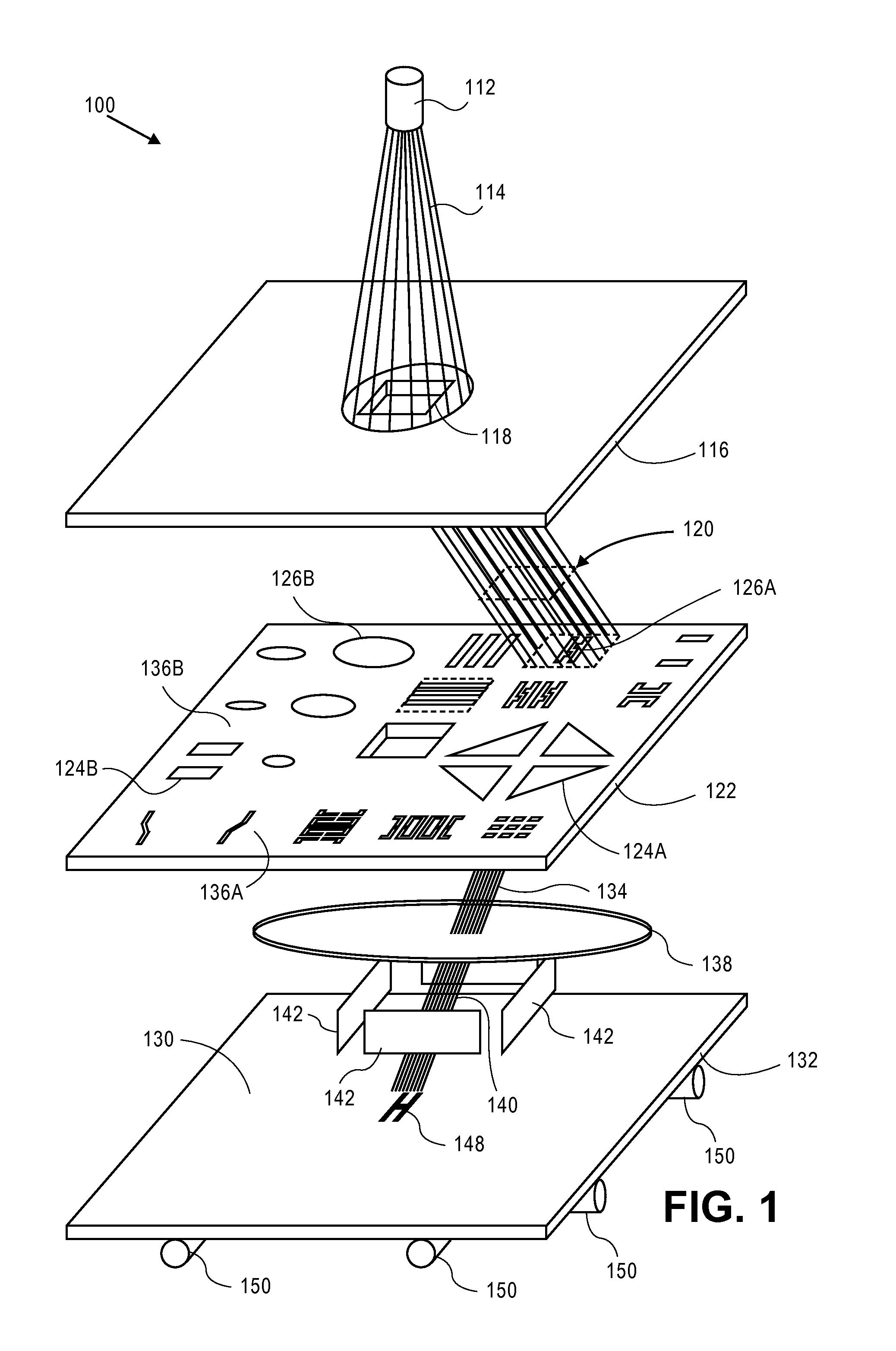
[0043]Referring now to the drawings, wherein like numbers refer to like items, FIG. 1 illustrates an embodiment of a conventional lithography system 100, such as a charged particle beam writer system, in this case an electron beam writer system, that employs character projection to manufacture a surface 130. The electron beam writer system 100 has an electron beam source 112 that projects an electron beam 114 toward an aperture plate 116. The plate 116 has an apertur...


PUM


Abstract

A method for manufacturing a semiconductor device is disclosed, wherein during the physical design process, a curvilinear path is designed to represent an interconnecting wire on the fabricated semiconductor device. A method for fracturing or mask data preparation (MDP) is also disclosed in which a manhattan path which is part of the physical design of an integrated circuit is modified to create a curvilinear pattern, and where a set of charged particle beam shots is generated, where the set of shots is capable of forming the curvilinear pattern on a resist-coated surface.

Description

RELATED APPLICATIONS[0001]This application claims priority from U.S. Provisional Patent Application Ser. No. 61 / 392,477, filed Oct. 13, 2010, entitled “Method For Integrated Circuit Manufacturing and Mask Data Preparation Using Curvilinear Patterns”; which is hereby incorporated by reference for all purposes.BACKGROUND OF THE DISCLOSURE[0002]The present disclosure is related to the manufacturing of integrated circuits, and more particularly to the use of curvilinear patterns for making photomasks.[0003]In the production or manufacturing of semiconductor devices, such as integrated circuits, optical lithography may be used to fabricate the semiconductor devices. Optical lithography is a printing process in which a lithographic mask or photomask manufactured from a reticle is used to transfer patterns to a substrate such as a semiconductor or silicon wafer to create the integrated circuit (I.C.). Other substrates could include flat panel displays, holographic masks, or even other reti...

Claims


Application Information

Patent Timeline
IPC IPC(8): G03F1/00G06F17/50
CPCG06F17/5077G06F2217/12G06F17/5081G03F7/70441G06F30/394G06F30/398G06F2119/18
Inventor FUJIMURA, AKIRATUCKER, MICHAEL
Owner D2S
Why Eureka
Try Eureka