Cmp polishing liquid and polishing method

a polishing liquid and polishing technology, applied in the direction of manufacturing tools, other chemical processes, chemistry apparatus and processes, etc., can solve the problems of difficult microfabrication of copper or copper alloy, difficult to achieve satisfactory polishing speed, and often deteriorated flatness, etc., to achieve favorable abrasive grain dispersion stability, high barrier film polishing speed, and rapid polishing of interlayer dielectrics

Active Publication Date: 2012-04-19
RESONAC CORP
View PDF8 Cites 33 Cited by
  • Summary
  • Abstract
  • Description
  • Claims
  • Application Information

AI Technical Summary

Benefits of technology

[0056]According to the present invention, since it is possible to obtain a CMT polishing liquid which attains a high barrier film polishing speed, has favorable abrasive grain dispersion stability, and is capable of rapidly polishing interlayer dielectrics, it is possible to improve a throughput by a reduction in polishing step time. Also, the polishing method according to the present invention, in which chemical mechanical polishing is performed by using the CMP polishing liquid, is suitably employed for producing semiconductor substrates and other electronic devices which have high productivity, excellent microfabrication, thin film formation, dimension accuracy, and electric property, and high reliability.

Problems solved by technology

However, it is difficult to perform microfabrication of copper or copper alloy by employing the dry etching method which has often been employed for conventional aluminum alloy wiring formation.
However, since a conductor used for the barrier film 2 has higher hardness as compared to the conductive material, it is difficult to attain a satisfactory polishing speed even when a polishing material for conductive material is used in combination, and the flatness is often deteriorated.

Method used


Image

  • Cmp polishing liquid and polishing method
  • Cmp polishing liquid and polishing method
  • Cmp polishing liquid and polishing method

Examples


first embodiment

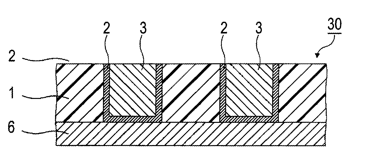
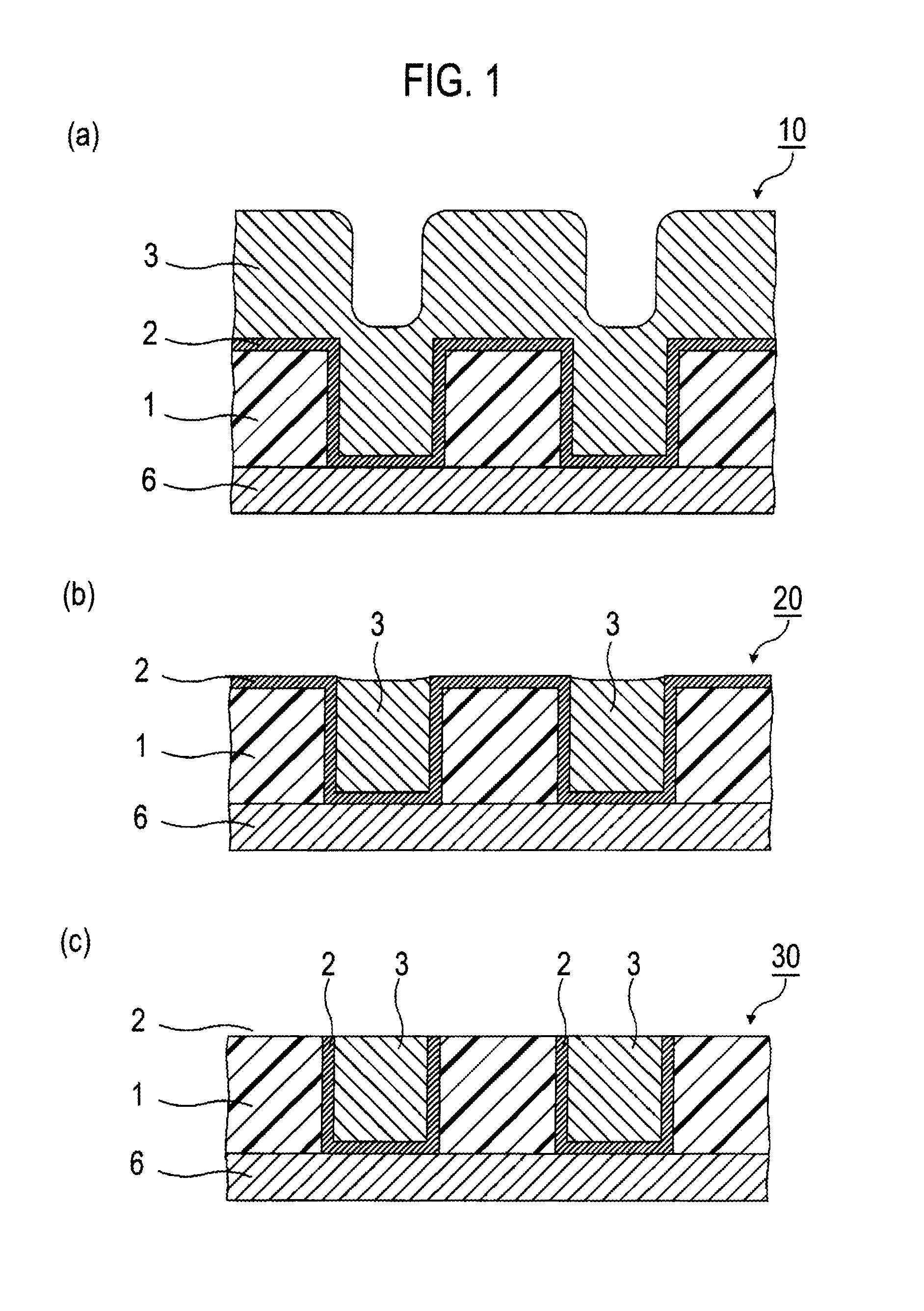
[0062]Hereinafter, CMP polishing liquids of the present invention will be orderly described. A first embodiment of the CMP polishing liquid of the present invention is a CMP polishing liquid which contains a medium and silica particles as an abrasive grain dispersed into the medium, wherein a silanol group density of the silica particles is 5.0 / nm2 or less; a biaxial average primary particle diameter when arbitrary 20 silica particles are selected from an image obtained by scanning electron microscope observation is 25 to 55 nm; and an association degree of the silica particles is 1.1 or more.

[0063]The CMP polishing liquid according to the first embodiment has favorable silica particle dispersion stability as compared to the conventional polishing liquid and is capable of attaining a favorable polishing speed for interlayer dielectrics. The reasons for the above-described effects have not been fully clarified, but the inventors assume as follows. Particles having a small silanol gro...

second embodiment

[0127]A second embodiment of the CMP polishing liquid of the present invention is a CMP polishing liquid containing a medium and silica particles as an abrasive grain dispersed into the medium, wherein the silica particles have the silanol group density of 5.0 / nm2 or less; the silica particles are not subjected to any surface treatment; the biaxial average primary particle diameter of the silica particles is 60 nm or less; and the association degree of the silica particles is 1.20 or less or between 1.40 and 1.80.

[0128]The CMP polishing liquid according to the second embodiment is capable of effectively suppressing occurrence of the seam which is the phenomenon that a thickness of interlayer dielectrics in the vicinity of the wiring metal part is decreased while attaining favorable polishing speeds fora barrier layer and the interlayer dielectrics. The reason for the achievement of the effect has not been fully clarified, but the inventors assume as follows.

[0129]As a mechanism for ...

examples

[0174]Hereinafter, the present invention will be described in conjunction with examples. However, the present invention is not limited by the examples.


PUM

PropertyMeasurementUnit
average primary particle diameteraaaaaaaaaa
zeta potentialaaaaaaaaaa

Abstract

The invention relates to a CMP polishing liquid comprising a medium and silica particles as an abrasive grain dispersed into the medium, characterized in that:(A1) the silica particles have a silanol group density of 5.0 / nm2 or less;(B1) a biaxial average primary particle diameter when arbitrary 20 silica particles are selected from an image obtained by scanning electron microscope observation is 25 to 55 nm; and(C1) an association degree of the silica particles is 1.1 or more. The invention provides a CMP polishing liquid which has the high barrier film polishing speed, the favorable abrasive grain dispersion stability, and the high interlayer dielectric polishing speed, and a polishing method producing semiconductor substrates or the like, that have excellent microfabrication, thin film formation, dimension accuracy, electric property and high reliability with low cost.

Description

TECHNICAL FIELD[0001]The present invention relates to a CMP polishing liquid and a polishing method to be used for polishing a semiconductor substrate wiring formation step and the like.BACKGROUND ART[0002]Microfabrication technologies have recently been developed in order to attain high integration and high performance of a semiconductor integrated circuit (hereinafter referred to as LSI). A chemical mechanical polishing (hereinafter referred to as CMP) method is one of the technologies, which is often used for flattening interlayer dielectrics, metal plug formation, and embedded wiring formation in a multilayer wiring formation step. The technology is disclosed in Patent Publication 1, for example.[0003]Also, in order to attain the high performance of LSI, use of copper or a copper alloy as a conductive material for a wiring material has recently been tried. However, it is difficult to perform microfabrication of copper or copper alloy by employing the dry etching method which has...

Claims


Application Information

Patent Timeline
Patent Type & Authority Applications(United States)
IPC IPC(8): H01L21/306
CPCC09G1/02H01L21/3212C09K3/1472C09K3/1463B24B57/02H01L21/304
Inventor KANAMARU, MAMIKOSHIMADA, TOMOKAZUSHINODA, TAKASHI
Owner RESONAC CORP
Why Eureka
Try Eureka