
Power semiconductor device

a technology of semiconductor devices and semiconductors, applied in the direction of transistors, basic electric elements, electric devices, etc., can solve the problems of difficult optimization for complete activation of dopant atoms, ion implantation process is well-known to generate life-time killing defects (crystalline damage), and limited sic mosfet developmen

Inactive Publication Date: 2012-04-26
UNIVSSENTERET PA KJELLER
View PDF1 Cites 3 Cited by
  • Summary
  • Abstract
  • Description
  • Claims
  • Application Information

AI Technical Summary

Problems solved by technology

The development of SiC MOSFETs is primarily limited by the low channel mobility and unreliability of the gate oxide.
The JFETs are normally-on devices and raise concerns for hybrid electric vehicle (HEV) applications due to the risk of driver supply voltage failure.
The base ion implantation process is well-known to generate life time killing defects (crystalline damage) in the bulk base region and surface region of SiC close to the base contact.
Also, ion implantation requires an extra high temperature annealing step for dopant activation, which is difficult to optimize for complete activation of dopant atoms.
Further, the use of a thin base layer of only 100 nm may pose a base punch through problem.
Also, precise control of such complex manufacturing processes is extremely difficult for the formation of a thin highly resistive p-type (HRP) layer within the emitter-base region in a lightly doped n-type SiC layer.
Generally speaking, the current gain (β) in SiC BJTs is primarily limited by the recombination of carriers at the surface, which still remains one of the critical issues for SiC BJT design.

Method used


Image

  • Power semiconductor device
  • Power semiconductor device
  • Power semiconductor device

Examples


Embodiment Construction

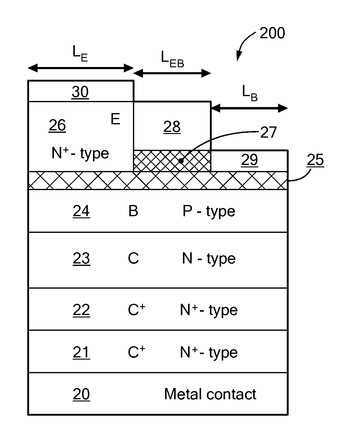
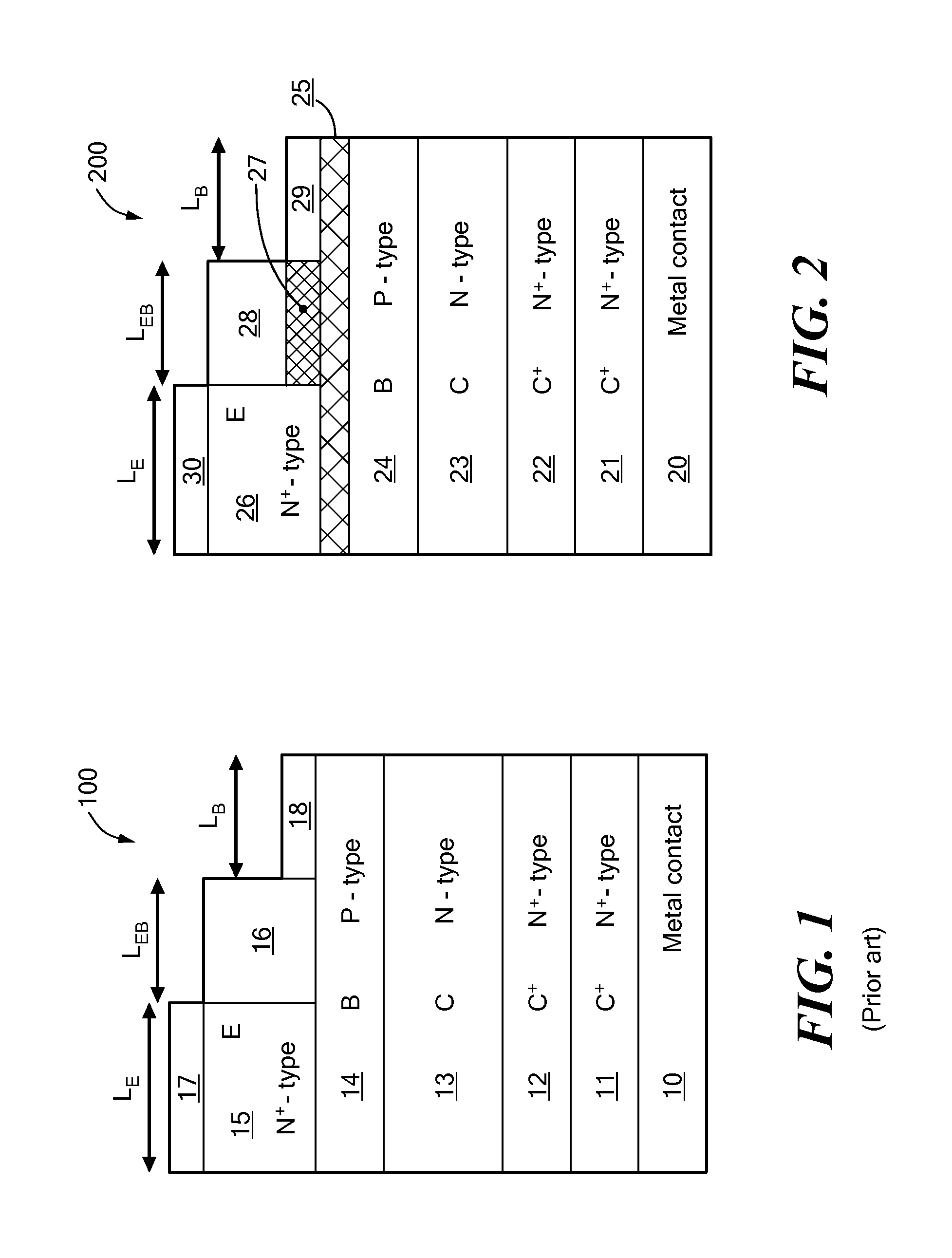
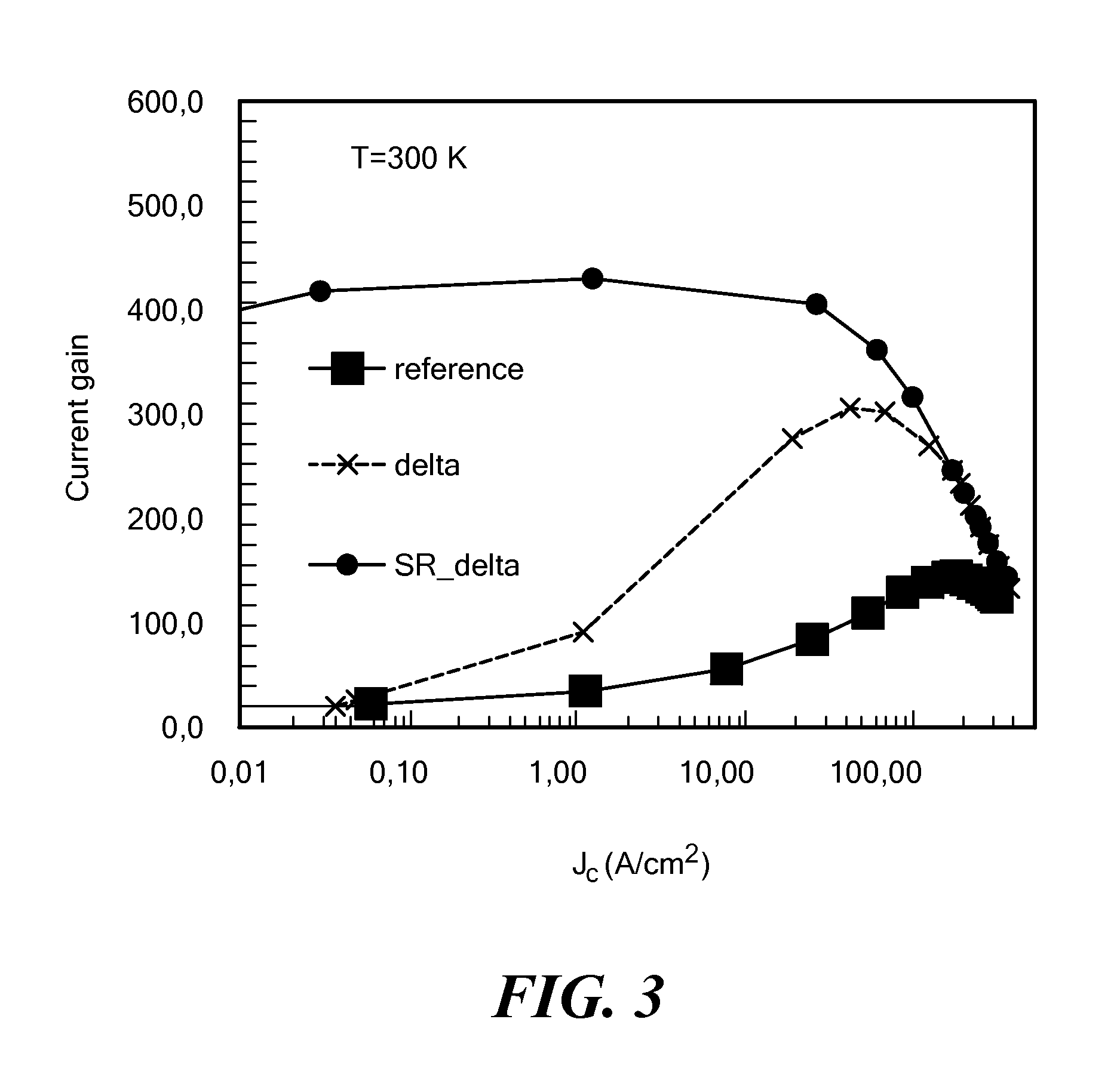
[0019]A method and apparatus for achieving high current gain, and low on-resistance, from a Bipolar Junction Transistor (BJT) in high temperature and high power applications are disclosed. In some embodiments, a thin doped delta layer is inserted at the base emitter junction but inside the base layer. In addition, in some embodiments, a surface recombination layer is inserted between the emitter-base regions of the device. In some embodiments, use of an ion implantation step is avoided to achieve simplicity and low cost of manufacture.

[0020]Before describing in detail exemplary embodiments that are in accordance with the present invention, it is noted that the embodiments reside primarily in combinations of apparatus components and processing steps related to bipolar transistor manufacture. Accordingly, the system and method components have been represented where appropriate by conventional symbols in the drawings, showing only those specific details that are pertinent to understand...


PUM


Abstract

A method and apparatus for achieving high current gain, and low on-resistance, from a Bipolar Junction Transistor (BJT) in high temperature and high power applications are disclosed. In some embodiments, a thin doped delta layer is inserted at the base emitter junction but inside the base layer. In addition, in some embodiments, a surface recombination layer is inserted between the emitter-base regions of the device. In some embodiments, use of an ion implantation step is avoided to achieve simplicity and low cost of manufacture.

Description

CROSS-REFERENCE TO RELATED APPLICATION[0001]n / aSTATEMENT REGARDING FEDERALLY SPONSORED RESEARCH OR DEVELOPMENT[0002]n / aFIELD OF THE INVENTION[0003]The present invention relates to a method and apparatus for achieving high current gain, and low on-resistance, from a Bipolar Junction Transistor (BJT) in high temperature and high power applications.BACKGROUND OF THE INVENTION[0004]Silicon carbide (SiC) based semiconductor electronic devices and circuits are presently being developed for use in high-temperature, high-power, and / or high-radiation conditions under which conventional semiconductors on a silicon (Si) substrate cannot adequately perform. Presently, most power electronics converter systems in automotive applications use silicon-(Si) based power semiconductor switches. The performance of these systems is approaching the theoretical limits of the fundamental material properties of the Si. The emergence of silicon carbide-(SiC) based power semiconductor switches likely will resu...

Claims


Application Information

Patent Timeline
Patent Type & Authority Applications(United States)
IPC IPC(8): H01L29/24H01L21/8222
CPCH01L21/8213H01L29/0804H01L29/0821H01L29/732H01L29/365H01L29/66068H01L29/73H01L29/1608
Inventor NAWAZ, MUHAMMAD
Owner UNIVSSENTERET PA KJELLER
Learn More