Lock in thermal laser stimulation through one side of the device while acquiring lock-in thermal emission images on the opposite side

a technology of thermal laser stimulation and lock-in thermal emission, which is applied in the field of defect localization analysis of semiconductor devices, can solve the problems of difficult to evenly fill the device with conductive material, difficult to test the device using traditional techniques, and localized heating of the chip

Active Publication Date: 2012-04-26
DCG SYST
View PDF6 Cites 18 Cited by
  • Summary
  • Abstract
  • Description
  • Claims
  • Application Information

AI Technical Summary

Problems solved by technology

One class of defects are those causing localized heating of the chip.
With the advancement in complex and stacked-die devices, it becomes increasingly difficult to test devices using traditional techniques.
Since TSV have high aspect ratio, it is difficult to evenly fill them with conductive material.
However, improperly filled TSV may lead to device performance degradation or even malfunction.

Method used


Image

  • Lock in thermal laser stimulation through one side of the device while acquiring lock-in thermal emission images on the opposite side
  • Lock in thermal laser stimulation through one side of the device while acquiring lock-in thermal emission images on the opposite side
  • Lock in thermal laser stimulation through one side of the device while acquiring lock-in thermal emission images on the opposite side

Examples


Embodiment Construction

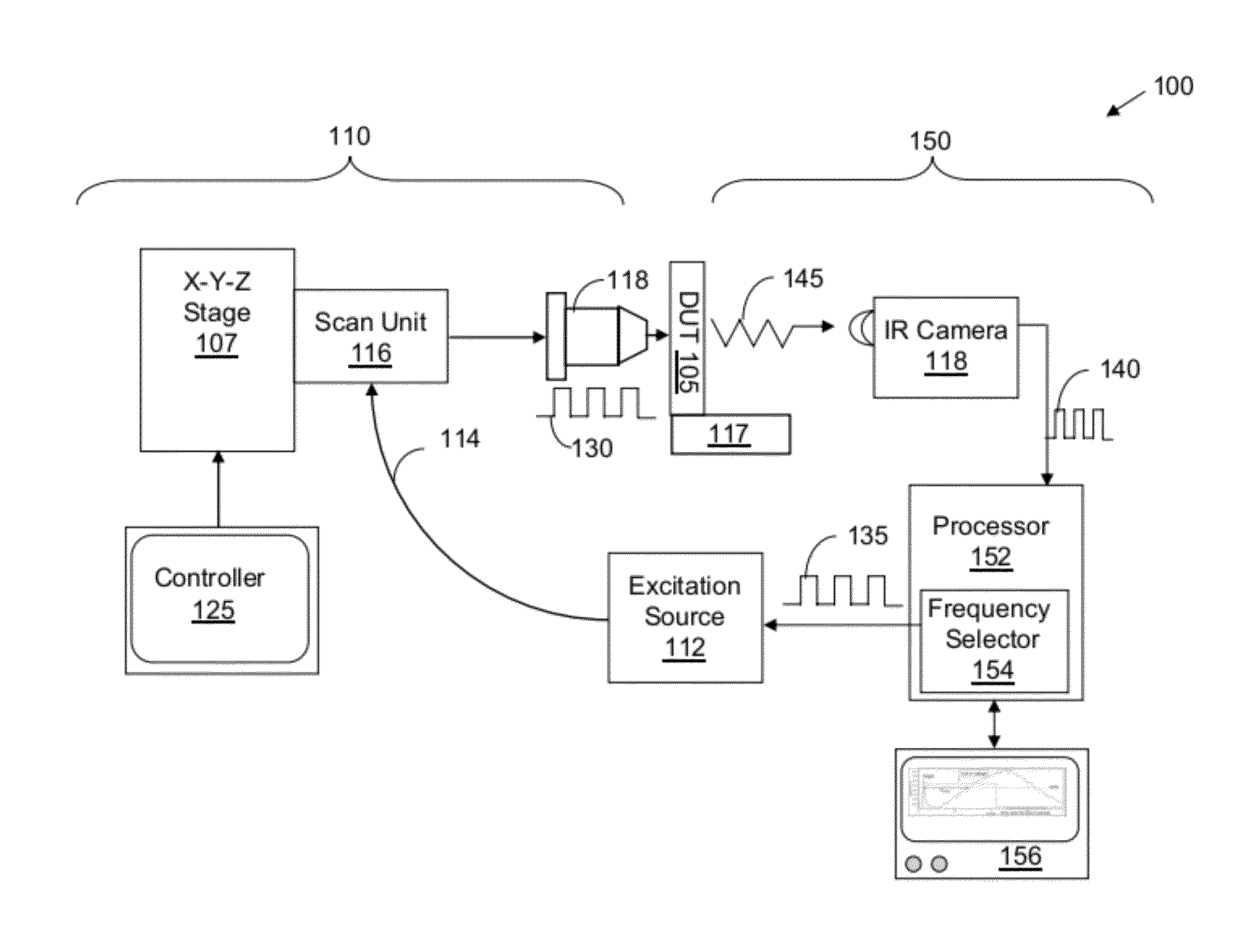
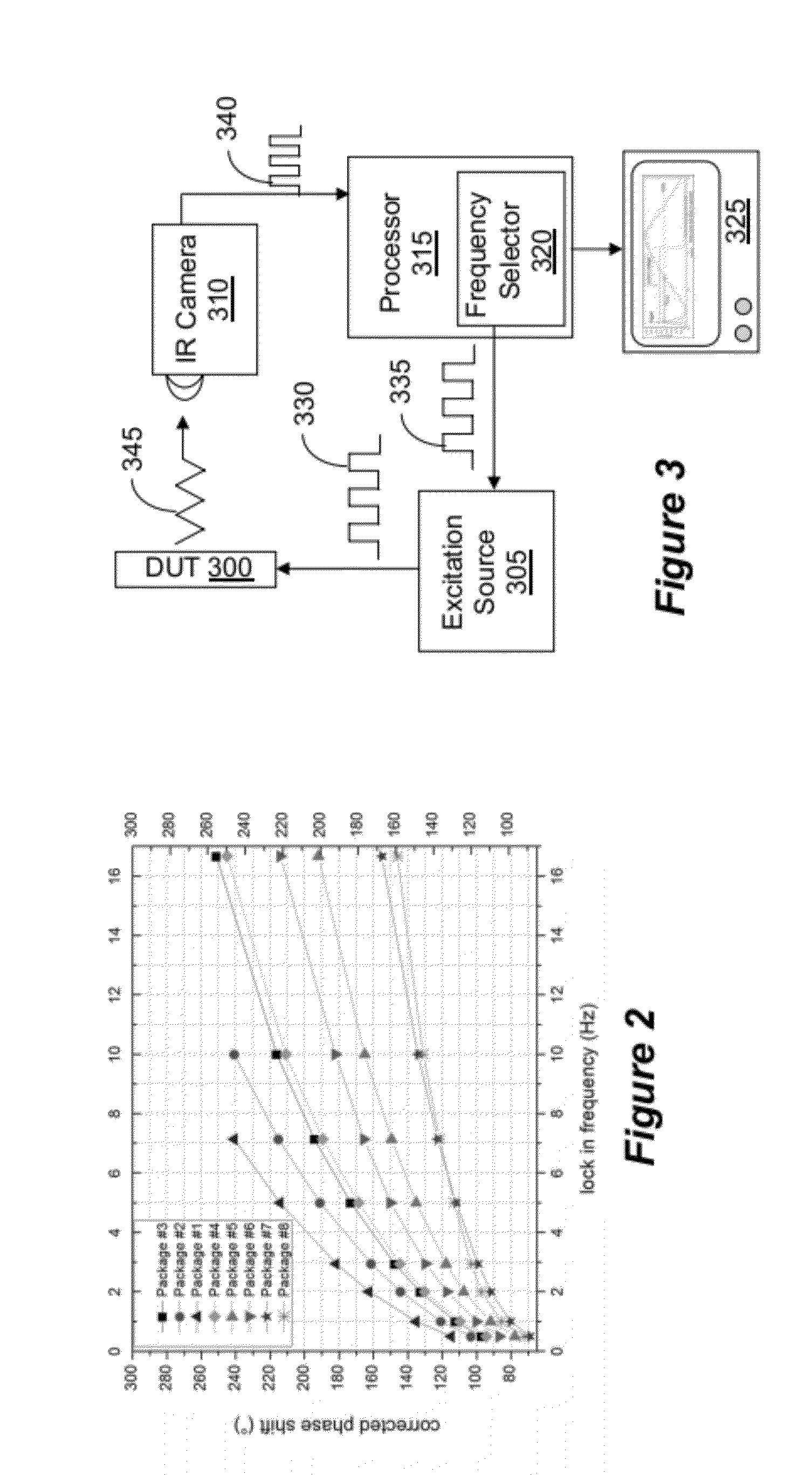
[0018]Embodiments of this invention enable thermal defect analysis using a micrometer spot size heat source and create calibration methods for IC's and stacked dies analysis. According to embodiments of the invention, light source, such as laser, laser diode, etc., is used to generate local heating inside the die. The local heating is studied using, e.g., thermal emission image acquisition from the opposite side of the die.

[0019]According to embodiments of the invention, the lock in thermal laser stimulation is combined along with the lock in thermal emission to study the IC design. One technique works from one side of the device and the other technique from the opposite side simultaneously and synchronously.

[0020]According to one embodiment, laser pulses (e.g., 1340 nm wavelength or any wavelength above 1064 nm, which is the silicon bandgap) are directed at a given location of the IC at a given lock-in frequency, thereby causing localized heating inside the IC. The optical system, ...


PUM


Abstract

Controlled amount of heat is injected into a stacked die using a light beam, and the propagated heat is measuring with LIT camera from the other side of the die. The thermal image obtained can be characterized so that it can be used to calibrate the phase shift from a given stack layer, or can be used to identify defects in the stacked die. The process can be repeated for each die in the stack to generate a reference for future testing. The thermal image can be investigated to detect faults, such as voids in vias, e.g., TSV.

Description

RELATED APPLICATIONS[0001]This Application claims priority benefit from U.S. Provisional Application Ser. No. 61 / 406,060, Filed Oct. 22, 2010, the disclosure of which is incorporated herein by reference in its entirety.BACKGROUND[0002]1. Field of Invention[0003]This invention is in the field of defect localization analysis of semiconductor devices and calibration apparatus and method for such defect localization.[0004]2. Related Art[0005]During design and verification stage of semiconductor devices, it is important to test for various defects or problematic areas of the chip design that may lead to defects. One class of defects are those causing localized heating of the chip. During the testing stage, it is important to identify such defects. One method for identifying localized heating defects is called Lock In Thermography (LIT). A current product available from the subject assignee, DCG Systems, Inc., of Fremont, Calif., uses this technique and is called ELITE™. The term LIT refe...

Claims


Application Information

Patent Timeline
Patent Type & Authority Applications(United States)
IPC IPC(8): H04N7/18
CPCG01N25/72G01R31/311H04N5/33G06T7/0008G01R35/005G06T7/001G01J5/0096G06T2207/10048G06T2207/30148G01J2005/0077
Inventor DESLANDES, HERVESCHLANGEN, RUDOLFSABBINENI, PRASADREVERDY, ANTOINE
Owner DCG SYST
Why Eureka
Try Eureka