Optoelectronic devices including heterojunction

a technology of heterojunction and optoelectronic devices, applied in the direction of semiconductor/solid-state device manufacturing, semiconductor devices, semiconductor devices, etc., can solve the problems of limiting the applications to which solar cells may be suited, preventing solar cells from becoming a mainstream energy source, and cost of producing solar cells, etc., to achieve higher bandgap, higher bandgap, and higher bandgap

Inactive Publication Date: 2012-05-03
ALTA DEVICES INC
View PDF2 Cites 28 Cited by
  • Summary
  • Abstract
  • Description
  • Claims
  • Application Information

AI Technical Summary

Benefits of technology

[0009]In one embodiment, an optoelectronic semiconductor device includes an absorber layer made of gallium arsenide (GaAs) and having only one type of doping. An emitter layer is located closer than the absorber layer to a back side of the device, the emitter layer made of a different material than the absorber layer and having a higher bandgap than the absorber layer. A heterojunction is formed between the emitter layer and the absorber layer, and a p-n junction is formed between the emitter layer and the absorber layer at a location offset from the heterojunction. The p-n junction causes a voltage to be generated in the device in response to the device being exposed to light at a front side of the device.
[0010]In another embodiment, a solar cell includes an absorber layer made of gallium arsenide (GaAs) and having only one type of doping, and an emitter layer made of a different material than the absorber layer and having a higher bandgap than the absorber layer. An intermediate layer is provided between the absorber layer and the emitter layer, the intermediate layer having the same type of doping as the absorber layer, wherein the intermediate layer includes a material gradation from GaAs at a side closer to the absorber layer, to the different material of the emitter layer at a side closer to the emitter layer. A heterojunction is formed between the emitter layer and the absorber layer, and a p-n junction is formed between the emitter layer and the absorber layer and at least partially within the different material at a location offset from the heterojunction. The p-n junction causes a voltage to be generated in the cell in response to the device being exposed to light at a front side of the solar cell.
[0011]In a

Problems solved by technology

Nevertheless, the currently high cost of producing solar cells relative to the low efficiency levels of contemporary devices is preventing solar cells from becoming a mainstream energy source and limiting the applications to which solar c

Method used


Image

  • Optoelectronic devices including heterojunction
  • Optoelectronic devices including heterojunction
  • Optoelectronic devices including heterojunction

Examples


Embodiment Construction

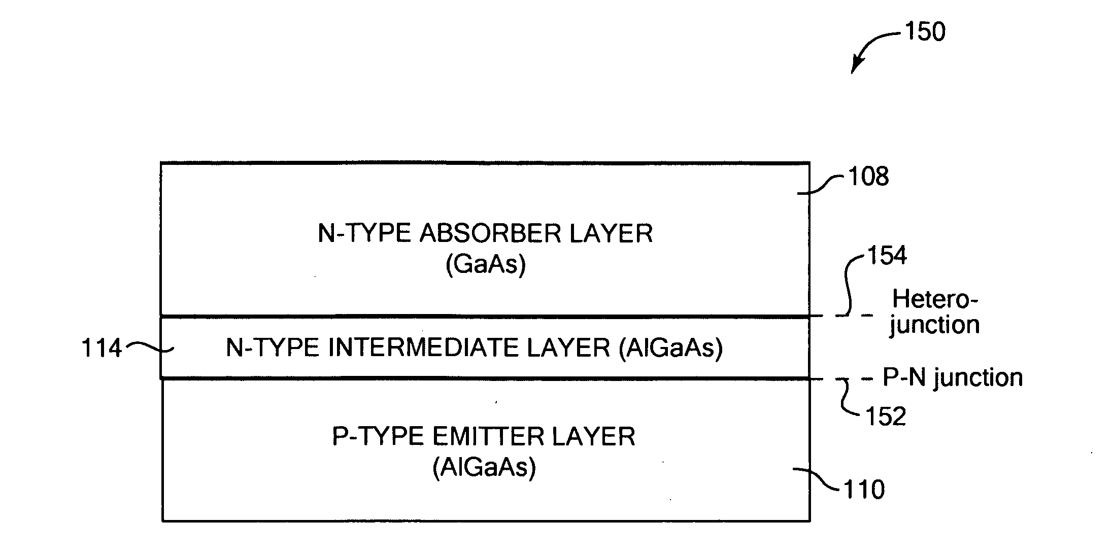
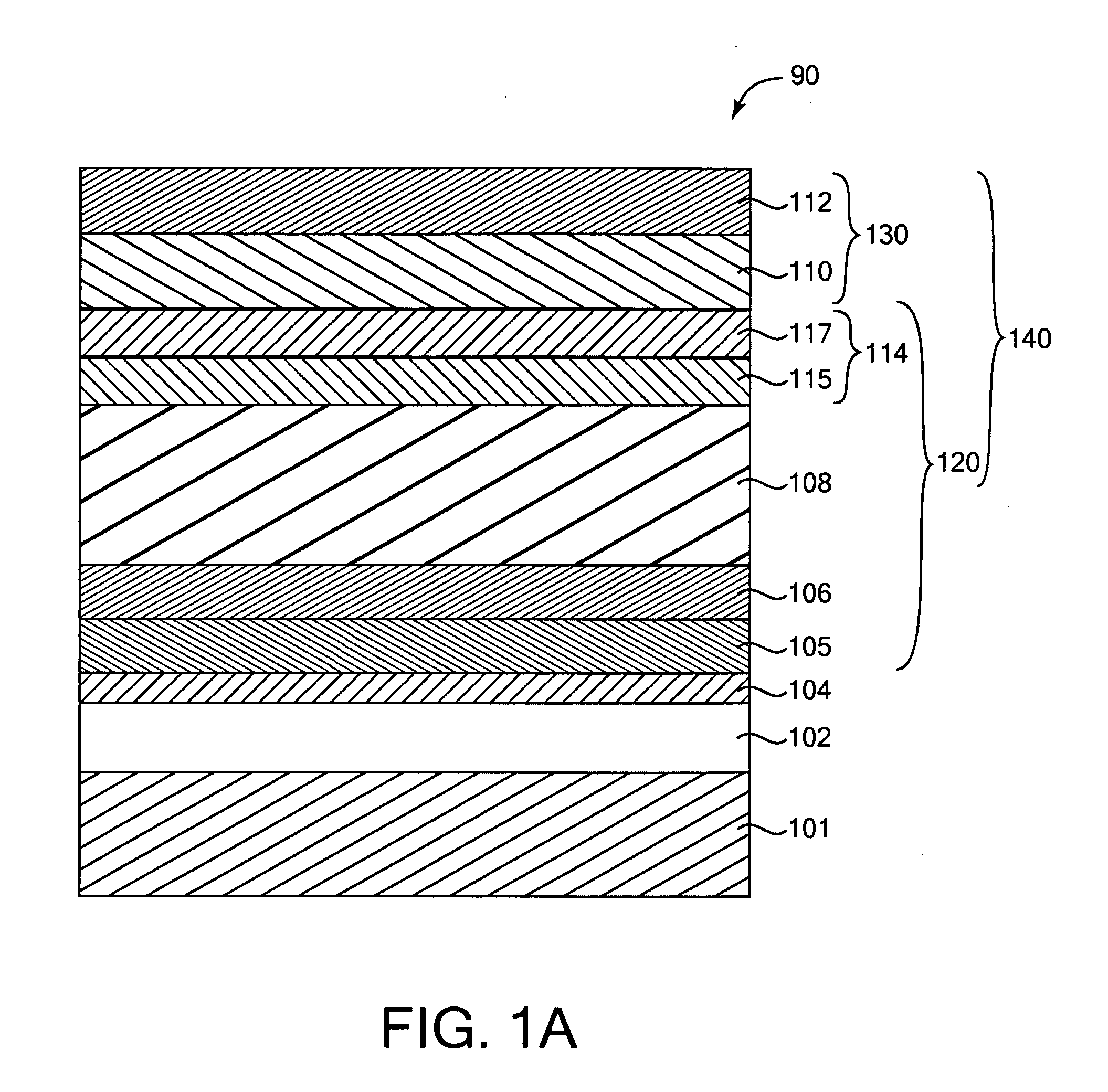
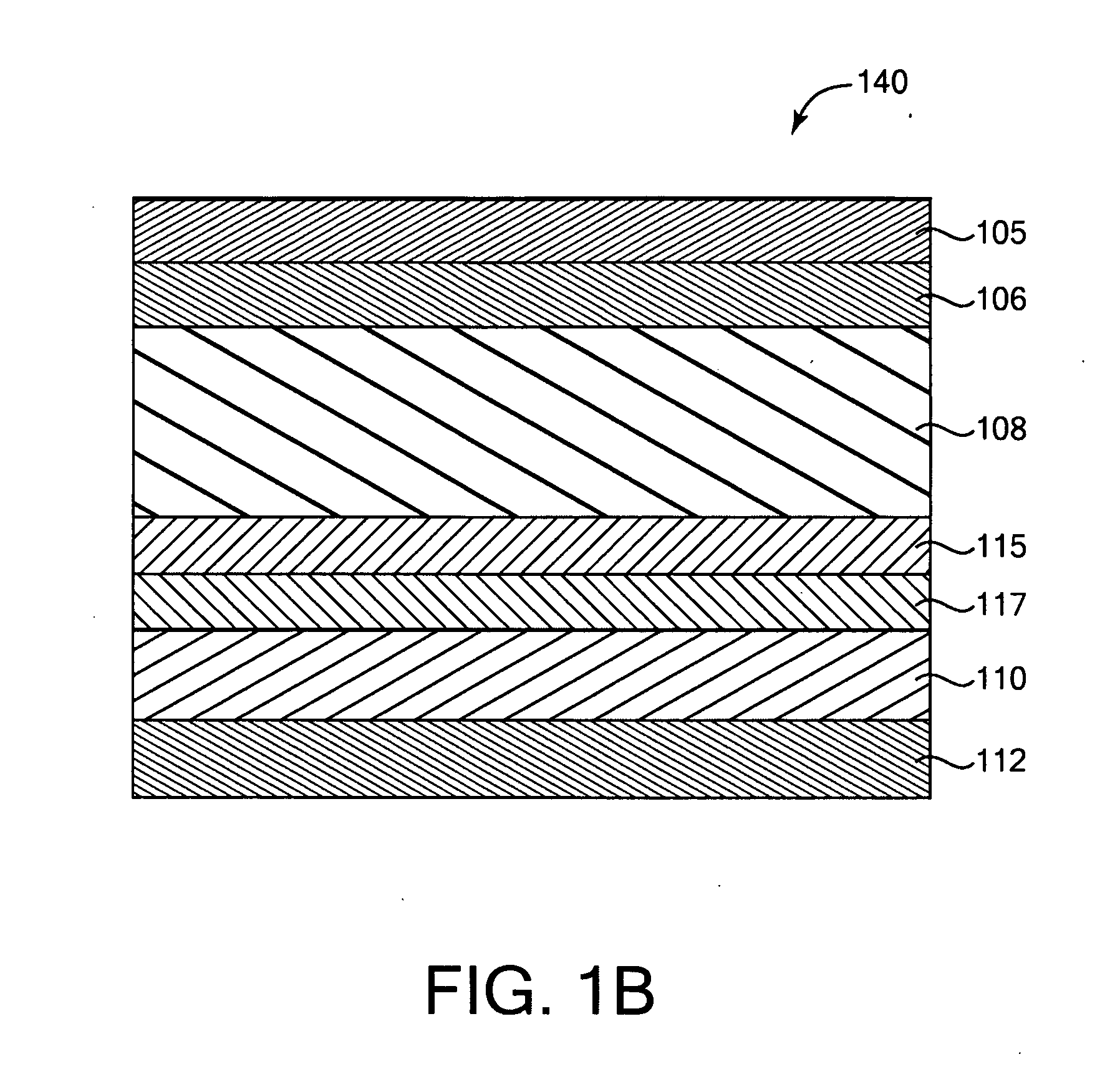
[0018]Embodiments of the invention generally relate to optoelectronic semiconductor devices and processes including photovoltaic devices and processes, and more specifically relate to photovoltaic cells and the fabrication processes for forming such photovoltaic cells and metallic contacts. Some of the fabrication processes include epitaxially growing thin films of gallium arsenide materials which are further processed by an epitaxial lift off (ELO) process. Some embodiments of photovoltaic cells described herein provide a gallium arsenide based cell containing an n-type film stack disposed over a p-type film stack, such that the n-type film stack is facing the front or sun side while the p-type film stack is on the back side of the cell. In one embodiment, the photovoltaic cell is a two-sided photovoltaic cell and has an n-metal contact disposed on the front side while a p-metal contact is disposed on the back side of the cell. In another embodiment, the photovoltaic cell is a sing...


PUM


Abstract

Embodiments of the invention generally relate to optoelectronic semiconductor devices such as photovoltaic devices including solar cells. In one aspect, an optoelectronic semiconductor device includes an absorber layer made of gallium arsenide (GaAs) and having only one type of doping. An emitter layer is located closer than the absorber layer to a back side of the device, the emitter layer made of a different material than the absorber layer and having a higher bandgap than the absorber layer. A heterojunction formed between the emitter layer and the absorber layer, and a p-n junction is formed between the emitter layer and the absorber layer and at least partially within the different material at a location offset from the heterojunction. The p-n junction causes a voltage to be generated in the device in response to the device being exposed to light at a front side of the device.

Description

BACKGROUND OF THE INVENTION[0001]1. Field of the Invention[0002]Embodiments of the invention generally relate to optoelectronic semiconductor devices such as photovoltaic devices including solar cells, and methods for fabricating such optoelectronic devices.[0003]2. Description of the Related Art[0004]As fossil fuels are being depleted at ever-increasing rates, the need for alternative energy sources is becoming more and more apparent. Energy derived from wind, from the sun, and from flowing water offer renewable, environment-friendly alternatives to fossil fuels, such as coal, oil, and natural gas. Being readily available almost anywhere on Earth, solar energy may someday be a viable alternative.[0005]To harness energy from the sun, the junction of a solar cell absorbs photons to produce electron-hole pairs, which are separated by the internal electric field of the junction to generate a voltage, thereby converting light energy to electric energy. The generated voltage can be incre...

Claims


Application Information

Patent Timeline
IPC IPC(8): H01L31/109H01L21/04
CPCH01L31/0735Y02E10/52H01L31/1896H01L31/022441Y02E10/544H01L31/0216H01L31/18H01L31/06H01L31/04
Inventor NIE, HUIKAYES, BRENDAN M.KIZILYALLI, ISIK C.
Owner ALTA DEVICES INC
Why Eureka
Try Eureka