Semiconductor laser device having inGaAs compressive-strain active layer, GaAsP tensile-strain barrier layers, and InGaP optical waveguide layers

Inactive Publication Date: 2002-09-05
NICHIA CORP +1
View PDF0 Cites 9 Cited by
  • Summary
  • Abstract
  • Description
  • Claims
  • Application Information

AI Technical Summary

Problems solved by technology

Therefore, in practice, temperature control is necessary, and thus cost reduction is difficult.
In the case that a semiconductor laser device having a layering structure as described above is driven under a high output condition, dark line failure due to the optical absorption by the laser facet, which has a plurality of surface states, and a phenomenon called facet

Method used


Image

  • Semiconductor laser device having inGaAs compressive-strain active layer, GaAsP tensile-strain barrier layers, and InGaP optical waveguide layers
  • Semiconductor laser device having inGaAs compressive-strain active layer, GaAsP tensile-strain barrier layers, and InGaP optical waveguide layers
  • Semiconductor laser device having inGaAs compressive-strain active layer, GaAsP tensile-strain barrier layers, and InGaP optical waveguide layers

Examples


first embodiment

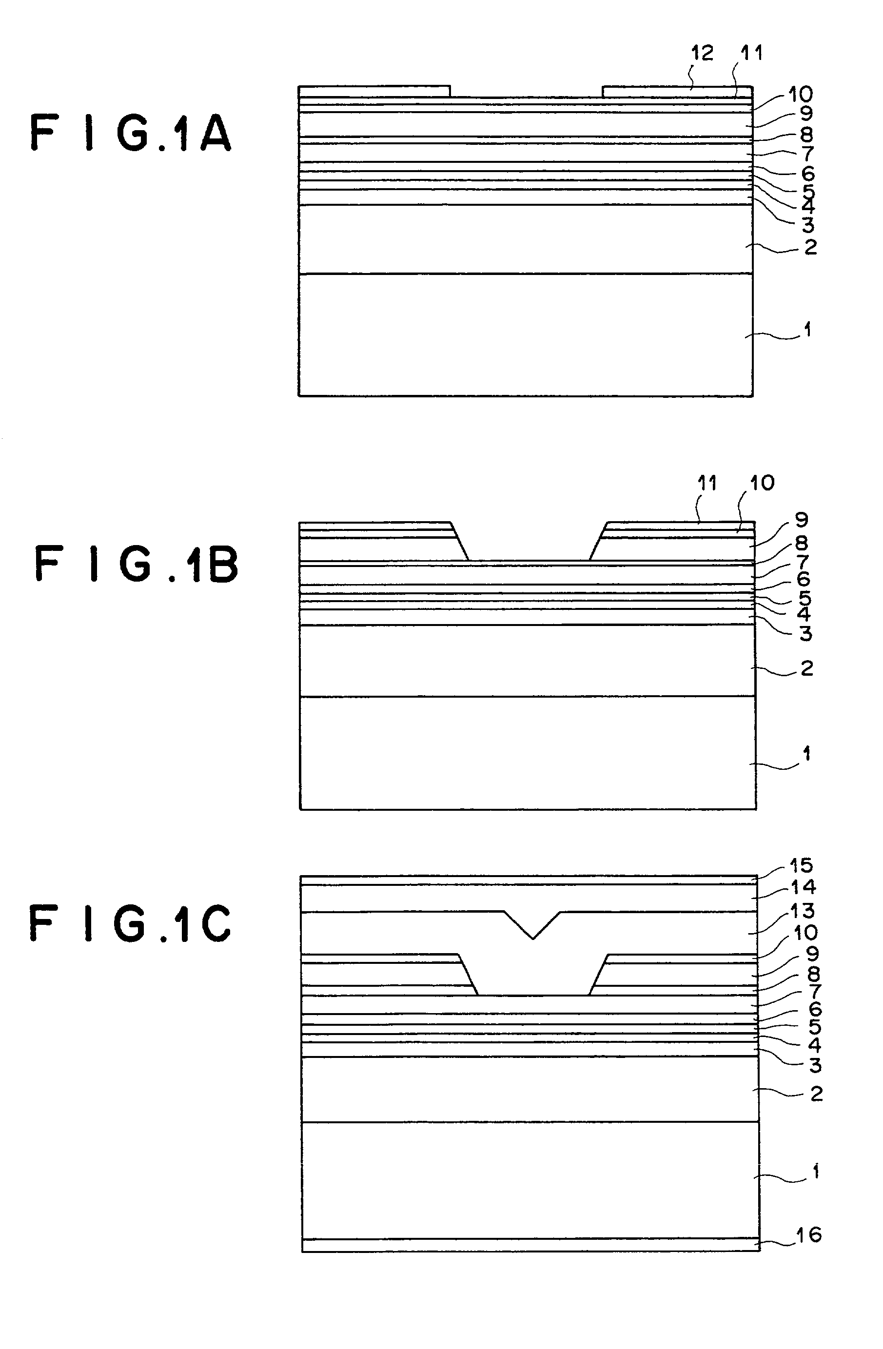
[0050] FIGS. 1A to 1C show cross sections of the representative stages in the process for producing a semiconductor laser device according to the first embodiment of the present invention.

[0051] First, as illustrated in FIG. 1A, an n-type Al.sub.z1Ga.sub.1-z1As lower cladding layer 2 (0.6.ltoreq.z1.ltoreq.0.8), an n-type or i-type (intrinsic) In.sub.0.49Ga.sub.0.51P lower optical waveguide layer 3, an In.sub.x2Ga.sub.1-x2As.sub.1-y2P.sub.1-y2 tensile-strain barrier layer 4 (0.ltoreq.x2<0.49y2 and 0

second embodiment

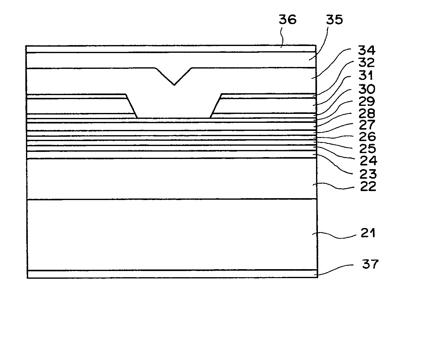
[0060] FIG. 3 is a cross-sectional view of a semiconductor laser device according to the second embodiment of the present invention.

[0061] First, as illustrated in FIG. 3, an n-type Al.sub.z1Ga.sub.1-z1As lower cladding layer 22 (0.6.ltoreq.z1.ltoreq.0.8), an n-type or i-type (intrinsic) In.sub.0.49Ga.sub.0.51P lower optical waveguide layer 23, an In.sub.x2Ga.sub.1-x2As.sub.1-y2P.sub.1-y2 tensile-strain barrier layer 24 (0.ltoreq.x2<0.49y2 and 0

third embodiment

[0068] FIG. 4 is a cross-sectional view of a semiconductor laser device according to the third embodiment of the present invention.

[0069] First, as illustrated in FIG. 4, an n-type Al.sub.z1Ga.sub.1-z1As lower cladding layer 42 (0.6.ltoreq.z1.ltoreq.0.8), an n-type or i-type (intrinsic) In.sub.0.49Ga.sub.0.51P lower optical waveguide layer 43, a GaAs.sub.1-y2P.sub.y2 tensile-strain barrier layer 44 (0


PUM


Abstract

In a semiconductor-laser device: a compressive-strain quantum-well active layer is made of Inx3Ga1. x3As1-y3Py3 (0<x3<=0.4 and 0<=y3<=0.1); tensile-strain barrier layers made of Inx2Ga1-2AS1-y2P1-y2 (0<=x2<0.49y2 and 0<y2<=0.4)are formed above and under the compressive-strain quantum-well active layer; and optical waveguide layers being made of either p-type or i-type In0.49Ga0.51P are formed above the upper tensile-strain barrier layer and under the lower tensile-strain barrier layer. Preferably, the absolute value of a sum of a first product and a second product is less than or equal to 0.25 nm, where the first product is a product of a strain and a thickness of said compressive-strain active layer, and the second product is a product of a strain of said lower and upper tensile-strain barrier layers and a total thickness of the lower and upper tensile-strain barrier layers.

Description

[0001] 1. Field of the Invention[0002] The present invention relates to a semiconductor laser device having a compressive-strain active layer.[0003] 2. Description of the Related Art[0004] M. Sagawa et al. ("High-power highly-reliable operation of 0.98-micrometer InGaAs-InGaP strain-compensated single-quantum-well lasers with tensile-strained InGaAsP barriers," IEEE Journal of Selected Topics in Quantum Electronics, Vol. 1, No. 2, 1995, pp.189) disclose semiconductor laser device which emits laser light in the 0.98-micrometer band without employing Al in any of its constituent layers. This semiconductor laser device is formed as follows.[0005] An n-type InGaP cladding layer, an undoped InGaAsP optical waveguide layer, an InGaAsP tensile-strain barrier layer, an InGaAs double-quantum-well active layer, an InGaAsP tensile-strain barrier layer, an undoped InGaAsP optical waveguide layer, a p-type InGaP first upper cladding layer, a p-type GaAs optical waveguide layer, a p-type InGaP se...

Claims


Application Information

Patent Timeline
IPC IPC(8): H01L21/205H01S5/20H01S5/223H01S5/34H01S5/343
CPCB82Y20/00H01S5/2081H01S5/2231H01S5/3403H01S5/3406H01S5/3434H01S5/34373
Inventor FUKUNAGA, TOSHIAKIOHGOH, TSUYOSHI
Owner NICHIA CORP
Why Eureka
Try Eureka