Flip-chip solar cell and manufacture method thereof

A solar cell and flip-chip technology, which is applied in the direction of circuits, photovoltaic power generation, electrical components, etc., can solve problems such as short-circuit current mismatch, and achieve the effects of increased thickness, improved tunneling effect, and improved bandgap

Active Publication Date: 2012-12-19
TIANJIN SANAN OPTOELECTRONICS
View PDF5 Cites 9 Cited by
  • Summary
  • Abstract
  • Description
  • Claims
  • Application Information

AI Technical Summary

Problems solved by technology

However, because the Ge bottom cell absorbs too many low-energy photons, it does not match the short-circuit current of the InGaP and GaAs top cells, so the traditional GaInP / GaAs / Ge triple-junction solar cell structure is not the most efficient combination.

Method used


Image

  • Flip-chip solar cell and manufacture method thereof
  • Flip-chip solar cell and manufacture method thereof
  • Flip-chip solar cell and manufacture method thereof

Examples


Embodiment 1

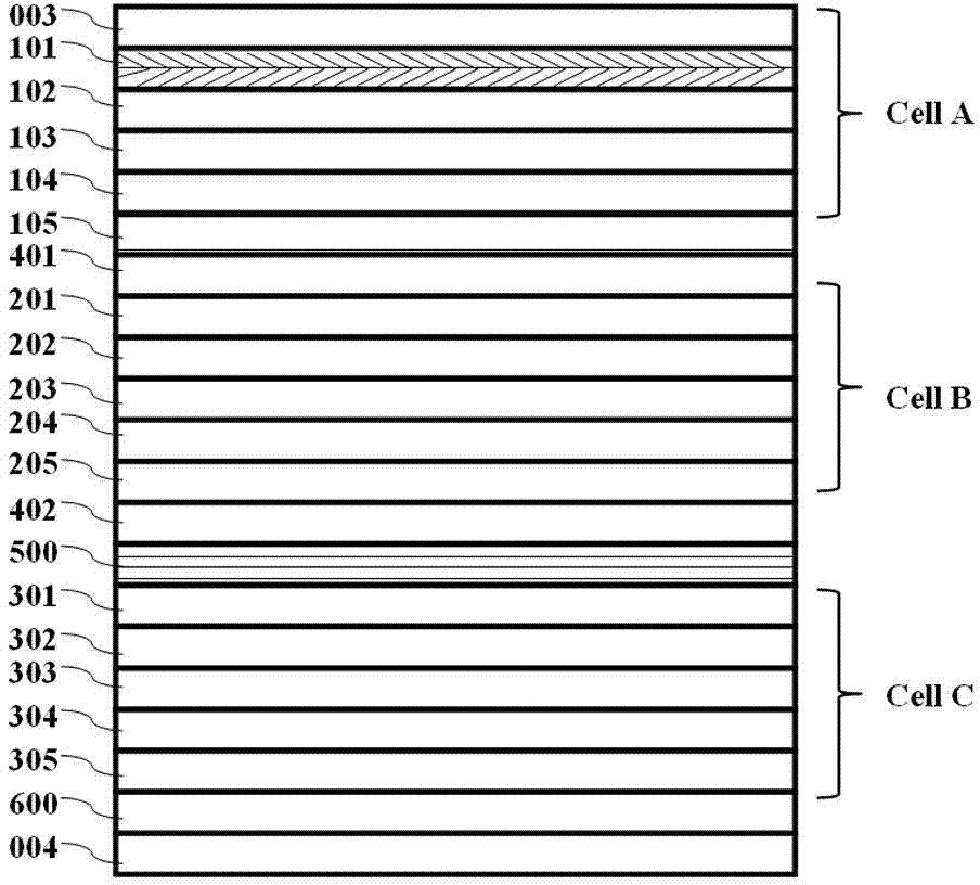
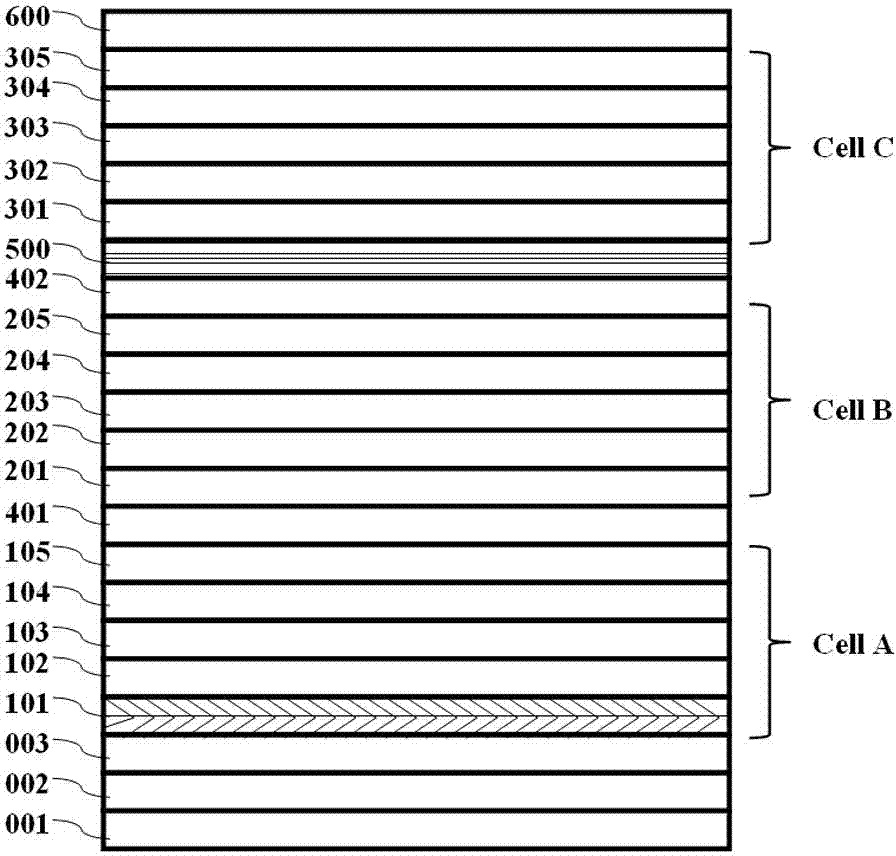
[0045] figure 1 Shown is an epitaxial structure of a flip-chip triple-junction solar cell, including from bottom to top: a growth substrate 001, an etching stop layer 002, an ohmic contact layer 3, a first GaInP sub-cell A, and a second GaAs sub-cell B 、In 0.3 GaAs third sub-cell C, capping layer 600, wherein each junction sub-cell is connected through tunnel junctions 401, 402, and a graded buffer layer 500 is used between the second and third sub-cells to solve the lattice mismatch between the two junction sub-cells. The structure will be described in detail below in conjunction with its preparation method.

[0046] Step 1: In the MOCVD system, the off-angle of n-type doping to the (111) crystal plane is selected as 9 0 The GaAs substrate is used as the growth substrate 001, the thickness is about 350 microns, and the doping concentration is 1×10 18 cm -3 ~4×10 18 cm -3 between. An InGaP etch stop layer 002 and a GaAs ohmic contact layer 003 are grown sequentially o...

Embodiment 2

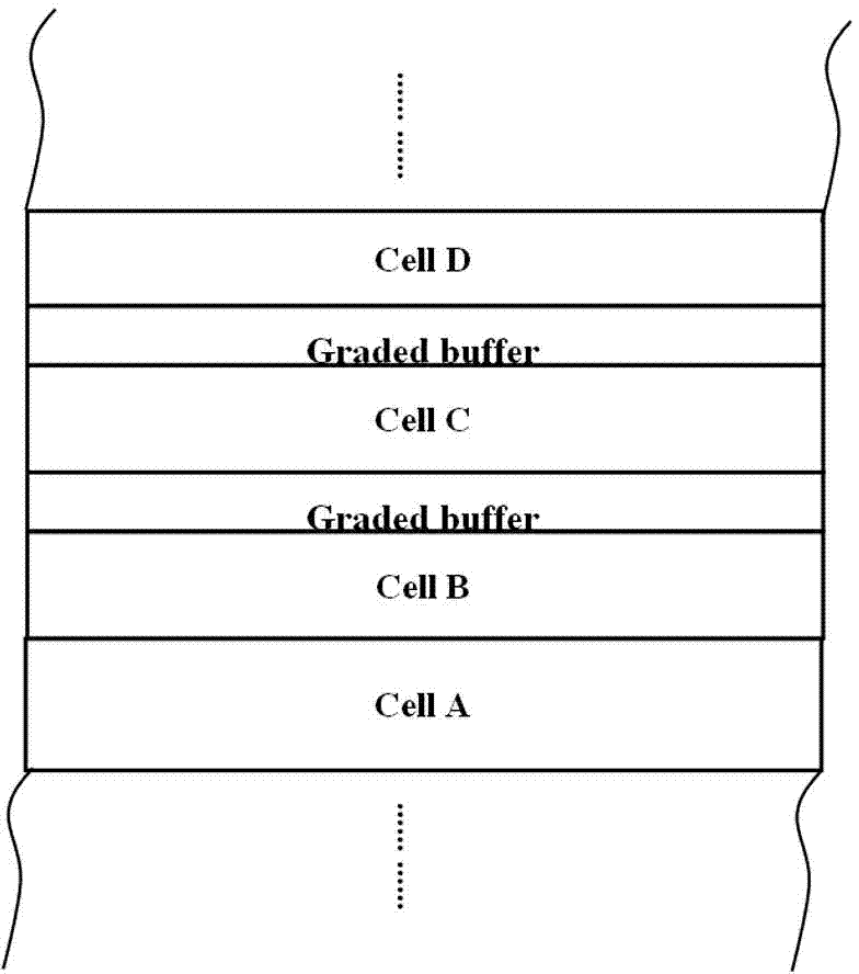
[0057] While satisfying the bandgap distribution as shown in Table 1, on the basis of Example 1, the epitaxial growth of the flip-chip four-junction solar cell (double graded buffer layer) can be continued, and its preparation mainly includes the following steps:

[0058] After implementing step 7 of Example 1, grow the tunnel junctions of the third and fourth subcells, and grow the second graded buffer layer InGaP, and grow 8 layers in total: including the stress release layer InxGa1-xP and the target lattice layer n+-In 0.737 Ga 0.263 P, where the stress release layer InxGa1-xP, the In composition of each layer increases from 0.737 to 1, and the corresponding lattice constant increases from 0.577 nm to 0.587 nm. The thickness of each layer was kept at 250 nm, and the doping concentration was 1×1018 cm-3. The last layer of the gradient buffer layer is the target lattice layer n+-In 0.737 Ga 0.263 P, its and the fourth sub-battery In 0.53 Ga 0.47 As has the same lattice ...

Embodiment 3

[0063] While satisfying the bandgap distribution as shown in Table 1, in the process of epitaxial growth of flip-chip triple-junction solar cells in Example 1, the Al(In)P / In(Ga)P superlattice structure is used instead of n+ - AlInP / InGaP heterojunction as the first sub-cell window 101, the thickness of each period is 10 nm, and the total thickness is 30 nm.


PUM


Abstract

The invention discloses a flip-chip solar cell and a manufacture method thereof. In a flip growing procedure of the flip-chip solar cell, a heterojunction window layer is imported in a top cell structure so as to prevent the window layer from being damaged by over etching which probably occurs in a manufacturing process, so that a serious consequence that the performance of the cell is influenced after a single-material window layer is damaged is avoided.

Description

technical field [0001] The invention relates to a flip-chip multi-junction solar cell and a preparation method thereof, belonging to the technical field of semiconductor materials. Background technique [0002] In recent years, solar cells have attracted more and more attention as a practical new energy source. It is a semiconductor device that uses the photovoltaic effect to convert solar energy into electrical energy, which greatly reduces people's dependence on coal, oil and natural gas in production and life, and has become one of the most effective ways to use green energy. In recent years, as the third-generation photovoltaic power generation technology, concentrating multi-junction compound solar cells have attracted much attention because of their high photoelectric conversion efficiency. [0003] Traditional GaInP / GaAs / Ge triple-junction solar cells have achieved a photoelectric conversion efficiency of over 41.8% under concentrating conditions. However, because ...

Claims


Application Information

Patent Timeline
Patent Type & Authority Applications(China)
IPC IPC(8): H01L31/0352H01L31/076H01L31/18
CPCY02E10/50Y02E10/548Y02P70/50
Inventor 毕京锋林桂江刘建庆丁杰
Owner TIANJIN SANAN OPTOELECTRONICS
Why Eureka
Try Eureka