Nano silicon window layer with gradient band gap characteristic and preparation method thereof

A nano-silicon and window layer technology, applied in nanotechnology, nanotechnology, nano-optics, etc., can solve the problems of difficult to obtain wide bandgap, i/p interface damage, interface bombardment damage, etc., to reduce interface carrier recombination , small particle bombardment, high conductivity effect

Inactive Publication Date: 2012-07-11
NANKAI UNIV
View PDF2 Cites 10 Cited by
  • Summary
  • Abstract
  • Description
  • Claims
  • Application Information

AI Technical Summary

Problems solved by technology

If the glow power is low, it is difficult to obtain a wide band gap; if the glow power is high, it is easy to cause bombardment damage to the interface, causing damage to the i / p interface in n-i-p amorphous silicon solar cells, reducing the solar cell performance
[0007] From the above analysis, it can be seen that p-type nano-silicon (nc-Si:H) as the window layer of amorphous silicon solar cells must solve two problems: 1) damage caused by high-energy particle bombardment during high-glow power deposition; 2) ) bandgap matching and bandgap transition between the wide bandgap window layer and the lower bandgap intrinsic layer

Method used


Image

  • Nano silicon window layer with gradient band gap characteristic and preparation method thereof
  • Nano silicon window layer with gradient band gap characteristic and preparation method thereof
  • Nano silicon window layer with gradient band gap characteristic and preparation method thereof

Examples


Embodiment 1

[0030] A preparation method of a nano-silicon window layer with gradient bandgap characteristics, comprising the following steps:

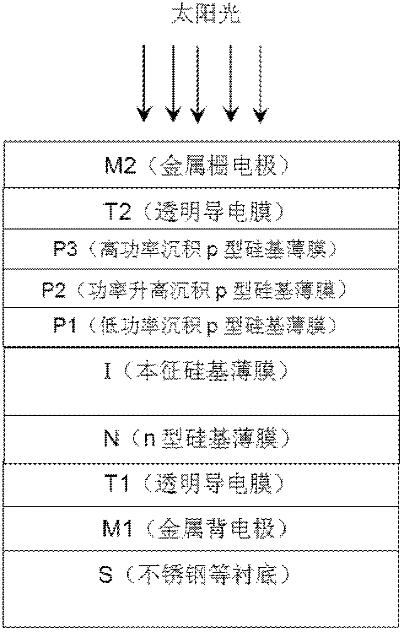
[0031] 1) Put the sample to be treated with the metal back electrode M, the transparent conductive back electrode T1, the n-type silicon-based film N and the intrinsic silicon-based film I stacked in sequence on the substrate into a plasma-enhanced chemical vapor phase of 13.56MHz-100MHz In the PECVD deposition equipment, the surface temperature of the sample to be processed is 150°C, and the background vacuum is 2×10 -4 Pa, into the reaction gas, the source gas in the reaction gas is silane SiH 4 ; The diluent gas is H 2 ; Doping gas is B 2 h 6 ; The ratio of dopant atoms to silicon atoms is 1%; the flow rate ratio of diluent gas to source gas is 250:1, the reaction gas pressure is 2Torr, and the glow power density is 0.08W / cm 2 A silicon film P1 with a thickness of 1.5nm was glow-deposited under the conditions;

[0032] 2) Change the glow p...

Embodiment 2

[0038] A preparation method of a nano-silicon window layer with gradient bandgap characteristics, comprising the following steps:

[0039] 1) Put the sample to be treated with the metal back electrode M, the transparent conductive back electrode T1, the n-type silicon-based film N and the intrinsic silicon-based film I stacked in sequence on the substrate into a plasma-enhanced chemical vapor phase of 13.56MHz-100MHz In the PECVD deposition equipment, the surface temperature of the sample to be processed is 150°C, and the background vacuum is 2×10 -4 Pa, into the reaction gas, the source gas in the reaction gas is silane SiH 4 ; The diluent gas is H 2 ; Doping gas is B 2 h 6 ; The ratio of dopant atoms to silicon atoms is 1%; the flow rate ratio of diluent gas to source gas is 250:1, the reaction gas pressure is 2Torr, and the glow power density is 0.08W / cm 2 A silicon film P1 with a thickness of 1.5nm was glow-deposited under the conditions;

[0040] 2) Change the glow p...


PUM

PropertyMeasurementUnit
thicknessaaaaaaaaaa
particle sizeaaaaaaaaaa
open-circuit voltageaaaaaaaaaa

Abstract

The invention relates to a nano silicon window layer with the gradient band gap characteristic, which is formed by depositing on the surface of a sample to be processed, wherein the surface of the sample to be processed is sequentially stacked with a metal back electrode M, a transparent conductive back electrode T1, an n-type Si-based thin film N and an intrinsic Si-based thin film I. The nano silicon window layer is formed by sequentially stacking a silicon thin film P1, a silicon thin film P2 and a silicon thin film P3. A preparation method of the nano silicon window layer comprises the following steps: depositing the p-type silicon thin film P1 with small thickness under a low glow power; then gradually raising the power and depositing the thin film P2; and finally, and completing the window layer P3 under a high power. The nano silicon window layer has the advantages that when the nano silicon window layer is applied to the window layer of an n-i-p-type silicon-based thin film solar cell, high electric conductance and wide band gap can be acquired, the bombardment of a solar cell i/p interface can be effectively reduced, the band gap matching between an intrinsic layer and the window layer can be implemented and the filling factor, the open-circuit voltage and the spectral response of the solar cell are obviously improved, so that the silicon-based thin film solar cell with high photoelectric conversion efficiency is obtained.

Description

technical field [0001] The invention relates to a silicon-based solar cell preparation process, in particular to a nano-silicon window layer with gradient band gap characteristics and a preparation method thereof. Background technique [0002] Solar cells are one of the effective ways to solve the increasingly severe environmental problems and energy supply problems. Due to the wide application of silicon materials in the semiconductor industry, and people have a very clear understanding of the various characteristics of silicon materials. Therefore, silicon-based solar cells occupy a very important position in all solar cells, among which solar cells related to amorphous silicon include amorphous silicon-based thin-film solar cells (including microcrystalline silicon and amorphous silicon germanium, etc.), and amorphous silicon-based solar cells HIT type heterojunction solar cells composed of crystalline silicon / monocrystalline silicon. [0003] Among silicon-based thin-f...

Claims


Application Information

Patent Timeline
Patent Type & Authority Applications(China)
IPC IPC(8): H01L31/075H01L31/0352H01L31/20B82Y40/00B82Y20/00C23C16/24C23C16/50
CPCY02E10/50Y02E10/548Y02P70/50
Inventor 侯国付倪牮马峻刘飞连张晓丹赵颖
Owner NANKAI UNIV
Why Eureka
Try Eureka