Optical modulator

a modulator and optical technology, applied in the field of optical modulators, can solve the problems of increasing the power consumption of the bias adjustment, increasing the power consumption of the driving circuit, and increasing the disadvantage of hybrid integrated-type nest mzi modulators, so as to eliminate the need for heat dissipation design/heat, the effect of reducing the chip cost of the pl

Active Publication Date: 2012-05-03
NIPPON TELEGRAPH & TELEPHONE CORP
View PDF10 Cites 18 Cited by
  • Summary
  • Abstract
  • Description
  • Claims
  • Application Information

AI Technical Summary

Benefits of technology

[0040]Furthermore, since there is no need to use the TO phase shifter, there is no need to form a thin film heater for example on the PLC. This provides an additional effect of reduced chip cost of the PLC. Furthermore, since the PLC includes no heat-generating section, another effect of eliminating the conventional need for a heat dissipation design / heat dissipation mechanism is obtained.

Problems solved by technology

However, the hybrid integrated-type nest MZI modulator had the disadvantage as shown below due to the use of the TO phase shifter.
Thus, a current output driving circuit is generally used, thus increasing the power consumption in the driving circuit.
As described above, in the hybrid integrated-type nest MZI modulator, a disadvantage was caused where high power consumption required for the bias adjustment was increased for both of a TO phase shifter as a relative phase adjusting section and a driving circuit as a relative phase adjusting section.

Method used


Image

  • Optical modulator
  • Optical modulator
  • Optical modulator

Examples


first embodiment

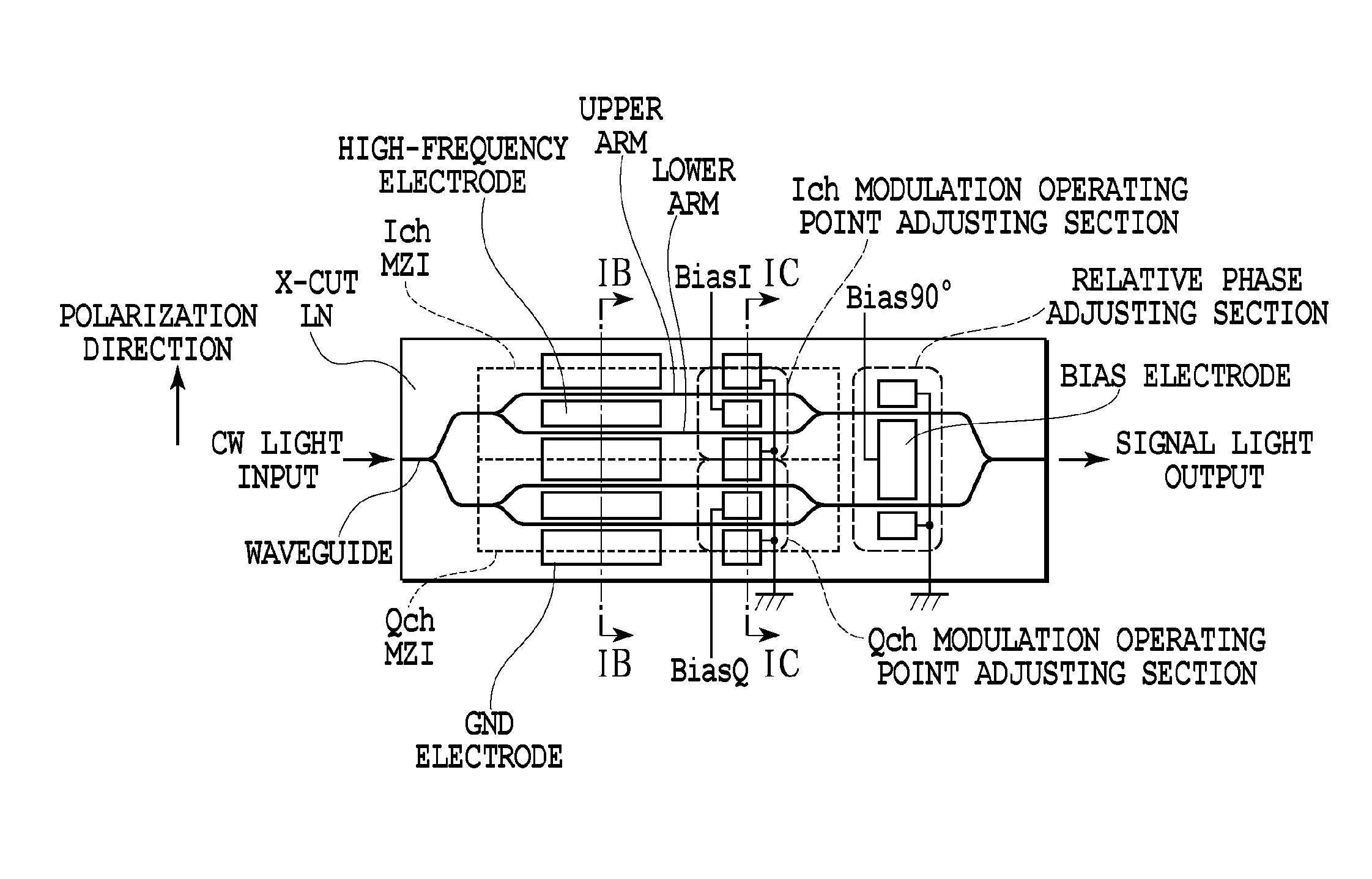
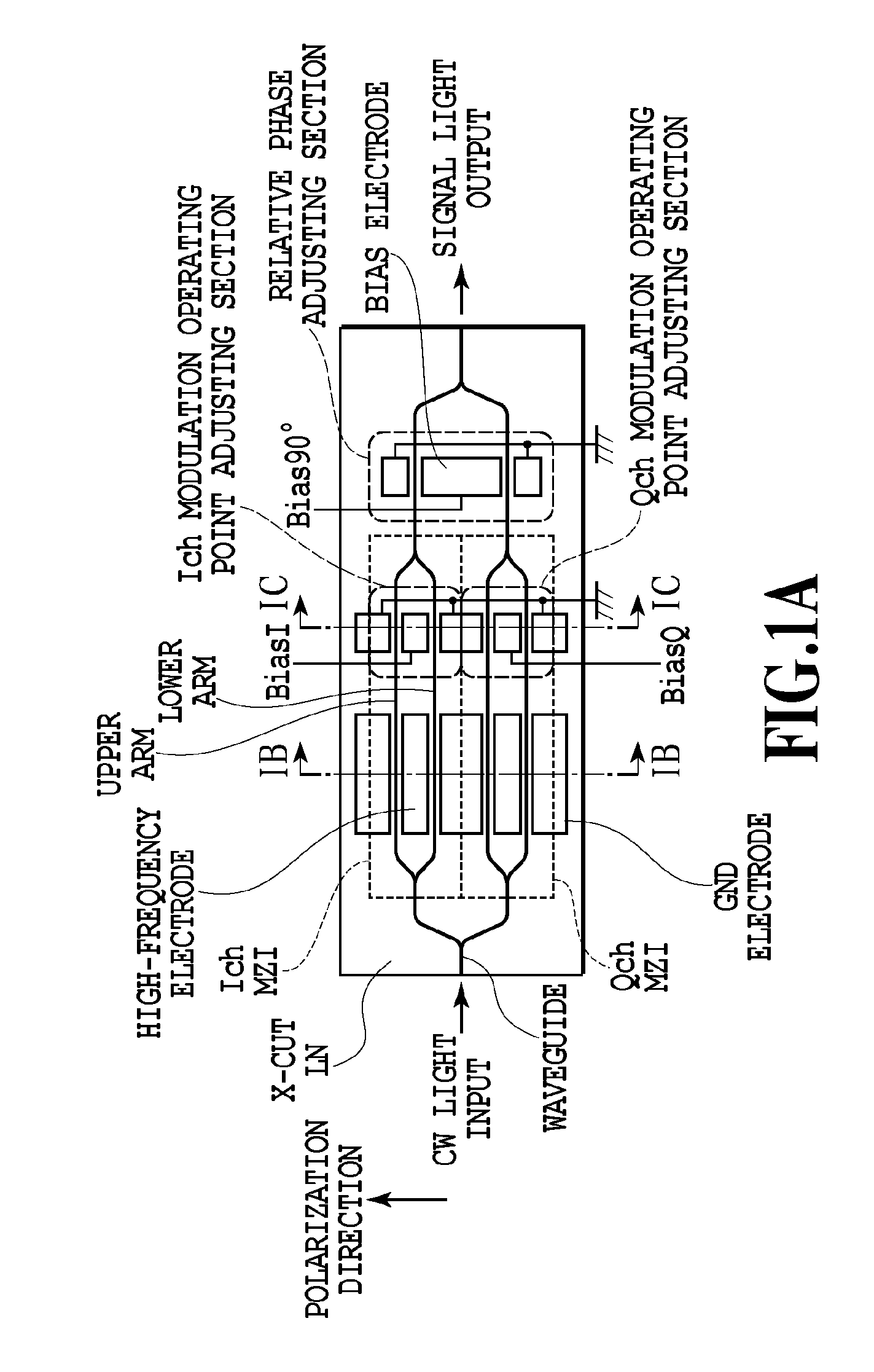
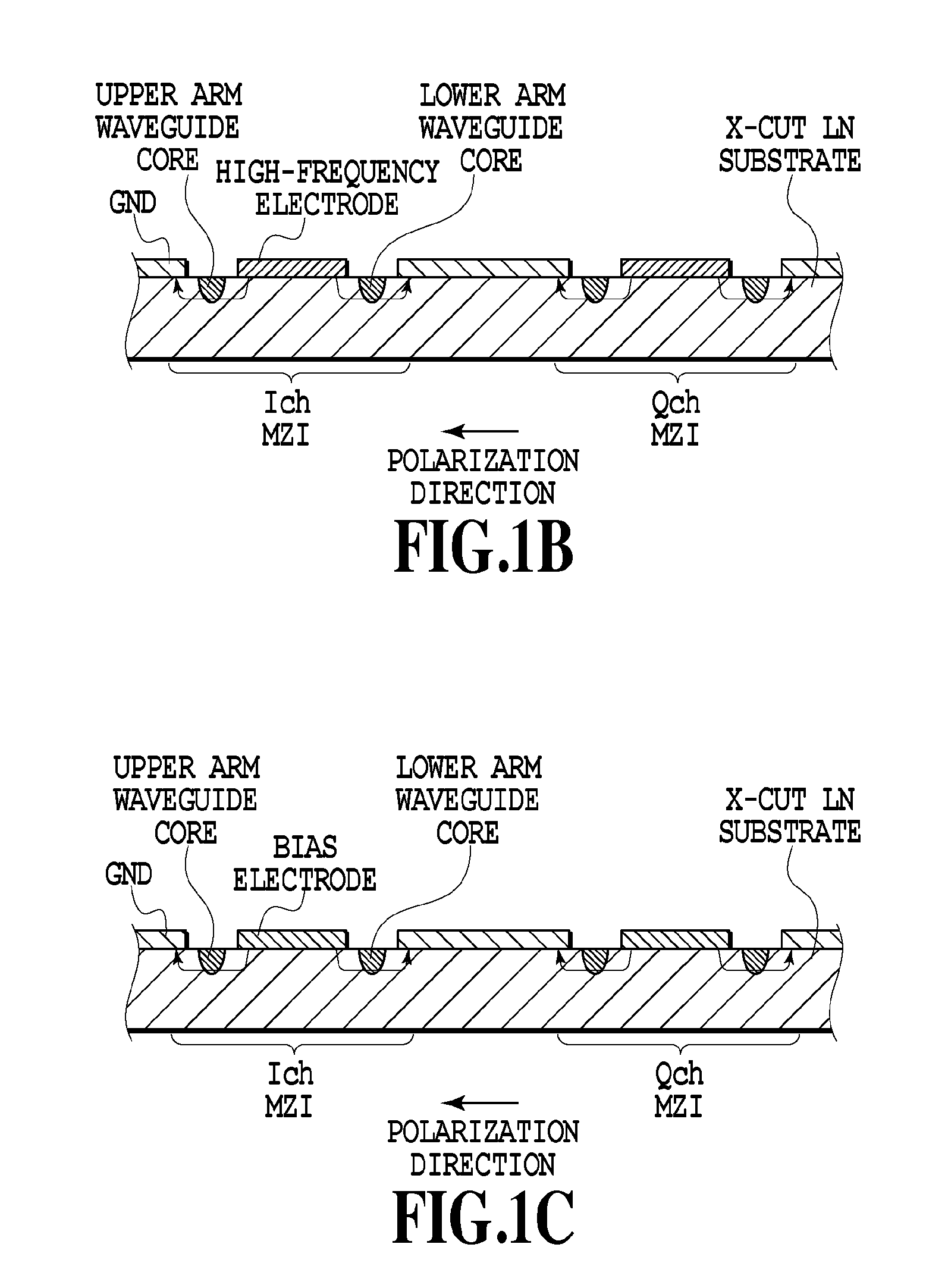
[0094]FIG. 4A illustrates the configuration of a hybrid integrated-type nest MZI modulator that is the first embodiment (embodiment 1a) of the invention of this application. The modulator configuration of this embodiment generally has the same configuration as the conventional one but is different in the relative phase adjusting section that adjusts the relative phase of an optical signal from a child MZI. Instead of providing a relative phase adjusting section in a parent MZI, each child MZI is allowed to include a bias electrode Bias90° (which corresponds to “first electrode”) in which both of the upper and lower arms receive an electric field in the same direction as the polarization direction (or an opposite direction) and a GND electrode (which corresponds to “second electrode”) (see FIG. 4B). The bias electrode Bias90° and the GND electrode provided in each child MZI constitute the entire relative phase adjusting section. The relative phase adjusting section as described above...

second embodiment

[0110]FIG. 7A illustrates the configuration of the hybrid integrated-type nest MZI modulator that is the second embodiment of the invention of this application (embodiment 2a). The configuration of this embodiment is significantly different in that the modulation operating point adjusting section and the relative phase adjusting section in the first embodiment are combined. Furthermore, each adjustment voltage was applied as the voltages V1, VQ, and V90 actually applied via the voltage dividing circuit with a resistance network to each bias electrode.

[0111]The function of the resistance r connected from each terminal to GND will be described later. Thus, the following section will firstly describe the operation of the circuit that is not connected to the resistance r. The resistance values of R1, R2, R3, and R4 are set to an identical value of R=R1=R2=R3=R4.

[0112]First, the following section will describe the 90° phase adjustment of the parent MZI. For simplicity, it is assumed that...

third embodiment

[0130]FIG. 10A illustrates the configuration of the hybrid integrated-type nest MZI modulator that is the third embodiment of the invention of this application. In this configuration, the modulation operating point adjusting section and the relative phase adjusting section include completely-independent electrodes so that electric fields applied to the respective arms of the respective MZI modulators can be individually controlled, which is different from the embodiments 1 and 2. A voltage actually applied to each electrode is digitally calculated as in the embodiment 2b. The voltages applied to the respective bias electrodes can be calculated by the following formulae.

VIH(p)=VbiasI+VBias90°

VIL(p)=−VBiasI+VBias90°

VQH(p)=VBiasQ−VBias90°

VQL(p)=−VBiasQ−VBias90°  Formula 7

VIH(n)=VBiasI−VBias90°

VIL(n)=VBiasI−VBias90°

VQH(n)=−VBiasQ+VBias90°

VQL(n)=VBiasQ+VBias90°  Formula 8

[0131]This configuration also uses the similar approach as in the embodiment 2b. Thus, the 90° phase adjustment of the...


PUM

PropertyMeasurementUnit
bending radiusaaaaaaaaaa
impedanceaaaaaaaaaa
terminating resistanceaaaaaaaaaa

Abstract

In a nest MZI modulator in which each arm includes a child MZI, the power consumption is reduced. The hybrid integrated-type nest MZI modulator of the embodiment 1a is configured so that, instead of placing a relative phase adjusting section in a parent MZI, a bias electrode Bias 90° in which an electric field is applied in the same direction to the polarization direction in both of the upper and lower arms is placed in each child MZI (see FIG. 4B). The bias electrode Bias 90° provided in each child MZI constitute the entirety of a relative phase adjusting section. The optical signals are subjected to a phase change after the output from the child MZI (see FIG. 1A), because such relative phase adjusting section can subject the optical signals of the upper and lower arms of the child MZI to a shift change in the same direction, respectively.

Description

TECHNICAL FIELD[0001]The present invention relates to an optical modulator. More particularly, the present invention relates to a nest MZI modulator.BACKGROUND ART[0002]In an optical fiber communication system, it has been considered to use a multilevel modulation technique and a polarization multiplexing technique in order to increase the transmission rate per one wavelength from 10 Gbps to 40 Gbps or 100 Gbps. The multilevel modulation technique is a technique that uses an optical signal amplitude together with phase information to transmit more many information in one symbol. With regard to 40 Gbps transmission, Differential Quadrature Phase-Shift Keying (DQPSK) modulation has been already used according to which four-state signal can be used to transmit 2-bit information per one symbol. The polarization multiplexing technique is a technique to use polarization to multiplex two types of signals to thereby obtain a doubled transmission rate. In the 100 Gbps-class transmission whic...

Claims


Application Information

Patent Timeline
Patent Type & Authority Applications(United States)
IPC IPC(8): G02F1/035
CPCG02B2006/12142G02B2006/12159G02F1/0327G02F1/225G02F2201/126G02F2203/20G02F2203/21
Inventor GOH, TAKASHIDOI, YOSHIYUKIMINO, SHINJITSUZUKI, KENYAMAZAKI, HIROSHIYAMADA, TAKASHI
Owner NIPPON TELEGRAPH & TELEPHONE CORP
Why Eureka
Try Eureka