Epitaxial silicon wafer and method for manufacturing same

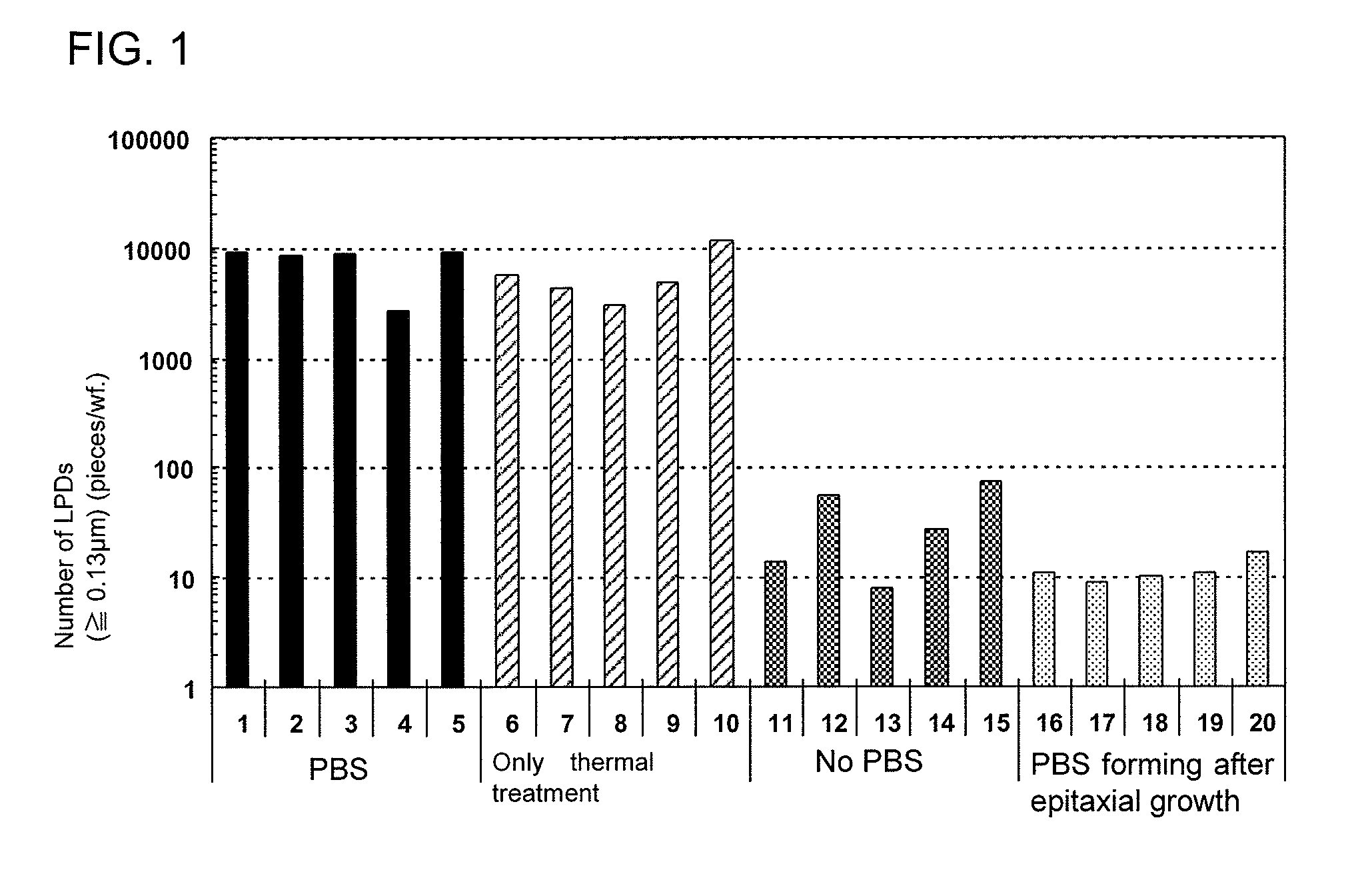
a silicon wafer and epitaxial technology, applied in the direction of coatings, semiconductor devices, chemical vapor deposition coatings, etc., can solve the problems of dislocation defect (a misfit dislocation) caused, difficult to manufacture a silicon crystal substrate with a required degree of resistivity, and difficulty in fully increasing the dopant concentration in a silicon crystal, etc., to achieve the effect of reducing the number of lpds on the surface of the silicon epitaxial layer

Active Publication Date: 2012-05-10
SUMCO CORP
View PDF3 Cites 7 Cited by
  • Summary
  • Abstract
  • Description
  • Claims
  • Application Information

AI Technical Summary

Benefits of technology

[0028]For the above method for manufacturing an epitaxial silicon wafer, a silicon epitaxial layer can be formed on the silicon crystal substrate at a temperature in the range of 1000 to 1090° C. in the t

Problems solved by technology

However, since the above dopant is extremely easily vaporized, it is difficult to fully increase a dopant concentration in a silicon crystal, whereby it is difficult to manufacture a silicon crystal substrate that is provided with a low resistivity that is a required degree.
However, in the case in which a silicon epitaxial layer is formed on a silicon crystal substrate into which phosphorus has been doped at a high concentration, a dislocation defect (a misfit dislocation) caused by a difference of a co

Method used


Image

  • Epitaxial silicon wafer and method for manufacturing same
  • Epitaxial silicon wafer and method for manufacturing same
  • Epitaxial silicon wafer and method for manufacturing same

Examples


Embodiment Construction

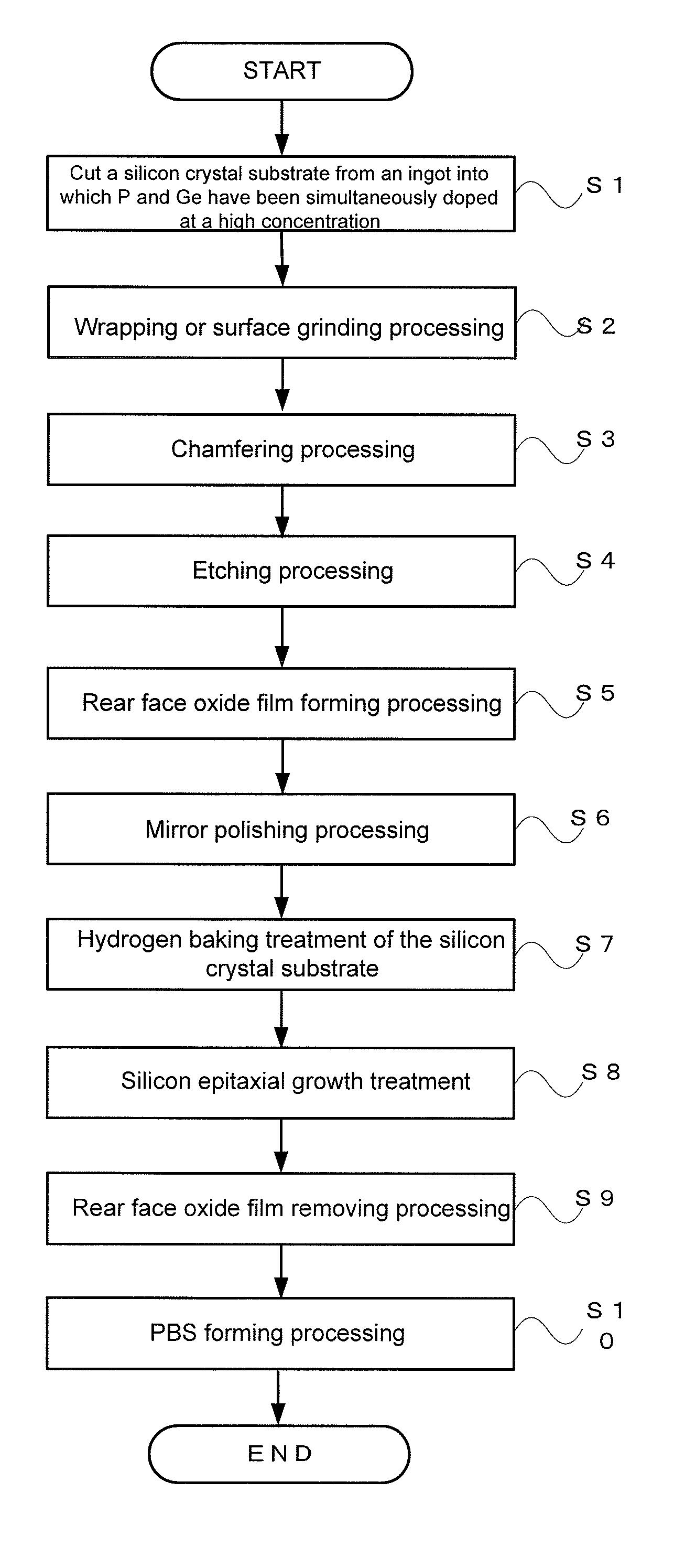
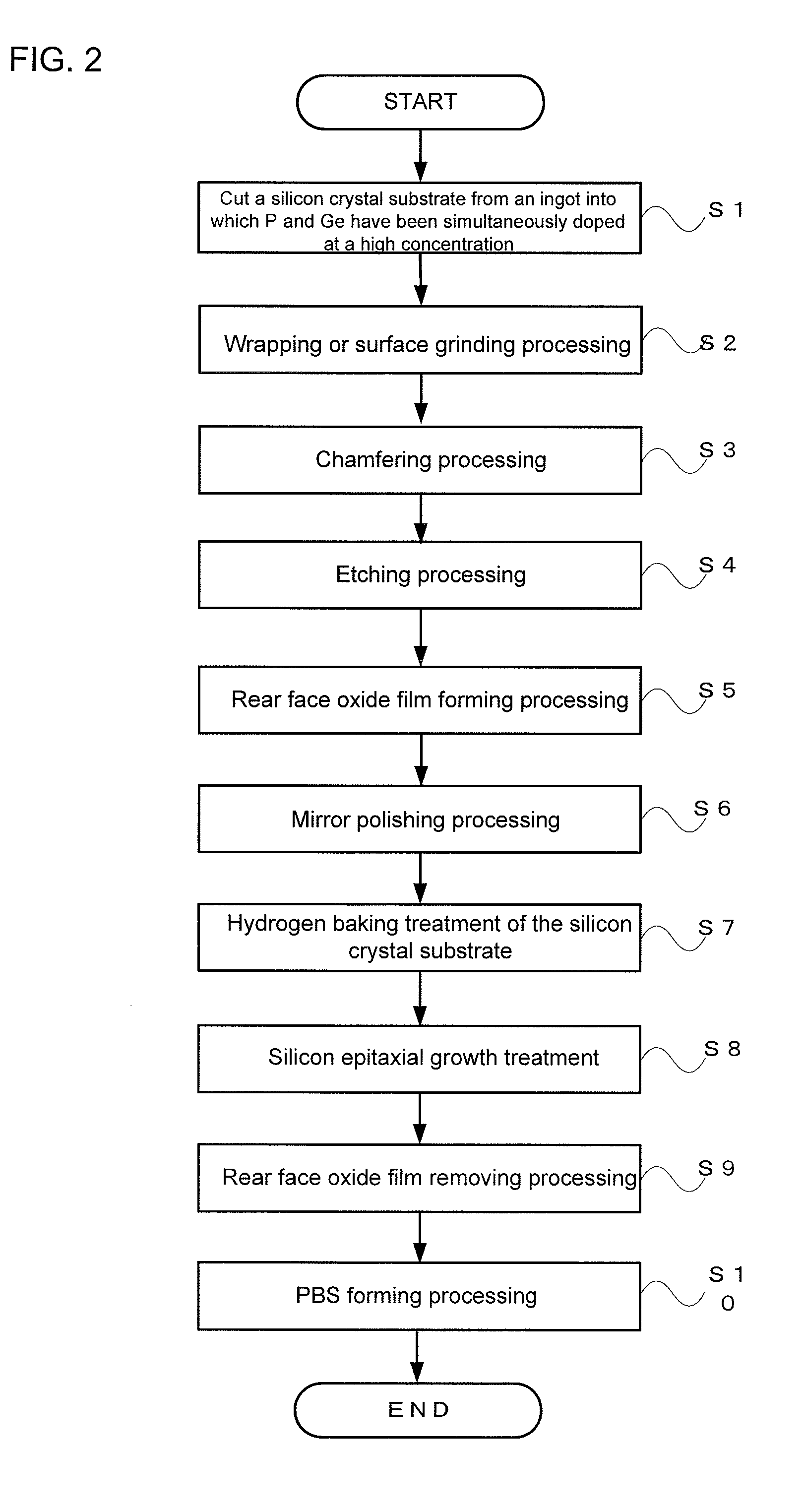
[0035]A method for manufacturing an epitaxial silicon wafer in accordance with the present invention will be described below in detail with reference to the drawings.

[0036]For the conventional technique as described above, after a polysilicon layer is formed on the rear face side of a silicon crystal substrate into which phosphorus (P) and germanium (Ge) have been doped in growing a silicon crystal (in particular, phosphorus and germanium have been doped at a high concentration that can implement an extremely low electric resistivity that is required for a power MOS transistor) (after the poly back seal forming treatment (PBS forming treatment) method), a silicon epitaxial layer is grown on the surface of the silicon crystal substrate. In that case, a number of stacking faults (SF) is generated in the silicon epitaxial layer.

[0037]The present inventors have found that an SF that is generated after an epitaxial growth is generated from a minute pit (a minute depressed part) as an ori...


PUM

PropertyMeasurementUnit
Temperatureaaaaaaaaaa
Areaaaaaaaaaaa
Concentrationaaaaaaaaaa

Abstract

It is an object to provide an epitaxial silicon wafer that is provided with an excellent gettering ability in which a polysilicon layer is formed on the rear face side of a silicon crystal substrate into which phosphorus (P) and germanium (Ge) have been doped. A silicon epitaxial layer is grown by a CVD method on the surface of a silicon crystal substrate into which phosphorus and germanium have been doped at a high concentration. After that, a PBS forming step for growing a polysilicon layer is executed on the rear face side of a silicon crystal substrate. By the above steps, the number of LPDs (caused by an SF) that occur on the surface of the epitaxial silicon wafer due to the SF can be greatly reduced.

Description

TECHNICAL FIELD [0001]The present invention relates to an epitaxial silicon wafer that is used for a semiconductor circuit and a method for manufacturing the epitaxial silicon wafer. More specifically, the present invention relates to an epitaxial silicon wafer in which a polysilicon layer is formed on the rear face side of a silicon crystal substrate into which phosphorus has been doped as an n-type dopant for adjusting an electric resistivity and germanium has been doped and a silicon epitaxial layer is formed on the surface of the silicon crystal substrate and to a method for manufacturing the epitaxial silicon wafer.BACKGROUND ART [0002]For instance, an electric resistivity of a silicon crystal substrate must be extremely low in the case of an epitaxial silicon wafer for a power MOS transistor. In order to reduce an electric resistivity of a silicon crystal substrate to a satisfactory extent, arsenic (As) and antimony (Sb) are doped as an n-type dopant for adjusting a resistivit...

Claims


Application Information

Patent Timeline
IPC IPC(8): H01L29/04H01L21/20
CPCH01L21/02381H01L21/02532H01L21/3221H01L21/02658H01L21/02664H01L21/0262
Inventor KAWASHIMA, TADASHIYOSHIKAWA, MASAHIROINOUE, AKIRAYOSHIDA, YOSHIYA
Owner SUMCO CORP
Why Eureka
Try Eureka