
Silicon-based suspending antenna with photonic bandgap structure

a technology of photonic bandgap and silicon-based suspension, which is applied in the direction of antennas, antenna details, coatings, etc., can solve the problems of narrow bandwidth and low radiation efficiency of planar antennas, errors in recognizing system data or affecting the overall efficiency of data sending and receiving, and narrow bandwidth and low radiation efficiency

Inactive Publication Date: 2012-05-10
IND TECH RES INST
View PDF12 Cites 2 Cited by
  • Summary
  • Abstract
  • Description
  • Claims
  • Application Information

AI Technical Summary

Problems solved by technology

In the conventional technology such as making a planar antenna on a PCB substrate, the planar antenna has a narrow bandwidth and low radiation efficiency.
In addition, due to the spurious wave effect and the surface effect of the microstrip antenna itself, when the conventional microstrip antenna in a communication system sends and receives signals, it can cause errors of the recognizing system data or affect the overall efficiency of data sending and receiving.
As to another conventional antenna, which is manufacturing on a silicon substrate (high dielectric constant), it has a narrow bandwidth and low radiation efficiency.

Method used


Image

  • Silicon-based suspending antenna with photonic bandgap structure
  • Silicon-based suspending antenna with photonic bandgap structure
  • Silicon-based suspending antenna with photonic bandgap structure

Examples


Embodiment Construction

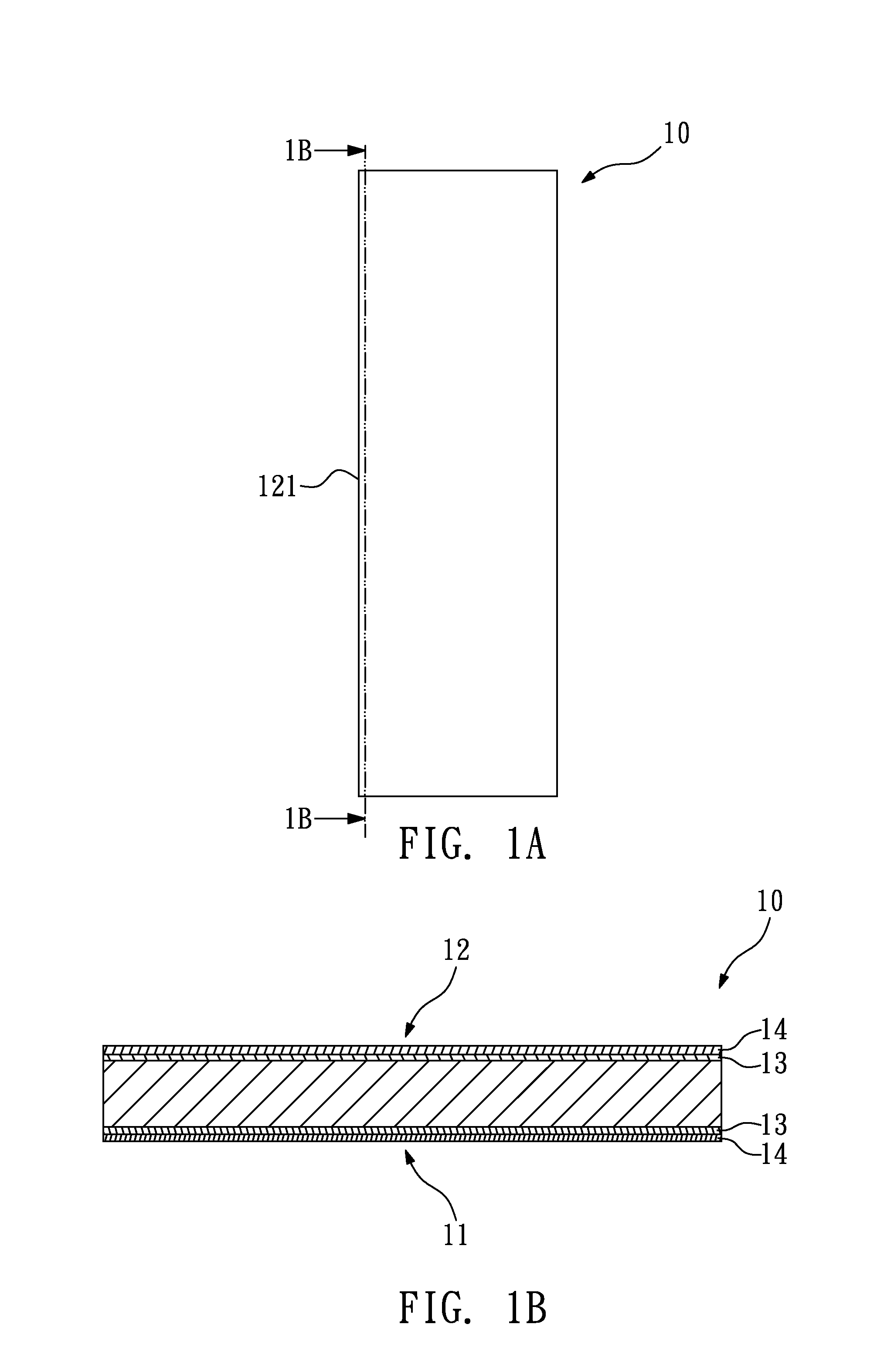
[0015]FIGS. 1A-9 show steps of making a silicon-based suspending antenna with photonic bandgap structure according to one embodiment of the disclosure. FIG. 1A is a top view of a silicon substrate according to one embodiment of the disclosure. FIG. 1B is a cross-sectional view along the cross-sectional line 1B-1B in FIG. 1A. As shown in FIGS. 1A and 1B, a silicon substrate 10 having a first side surface 11 and a second side surface 12 oppositing to the first surface 11 is provided, wherein the second side surface 12 has a longitudinal edge 121. In this embodiment, the first side surface 11 and the second side surface 12 have a silicon dioxide layer 13 and a nitride layer 14 from inside to outside, respectively.

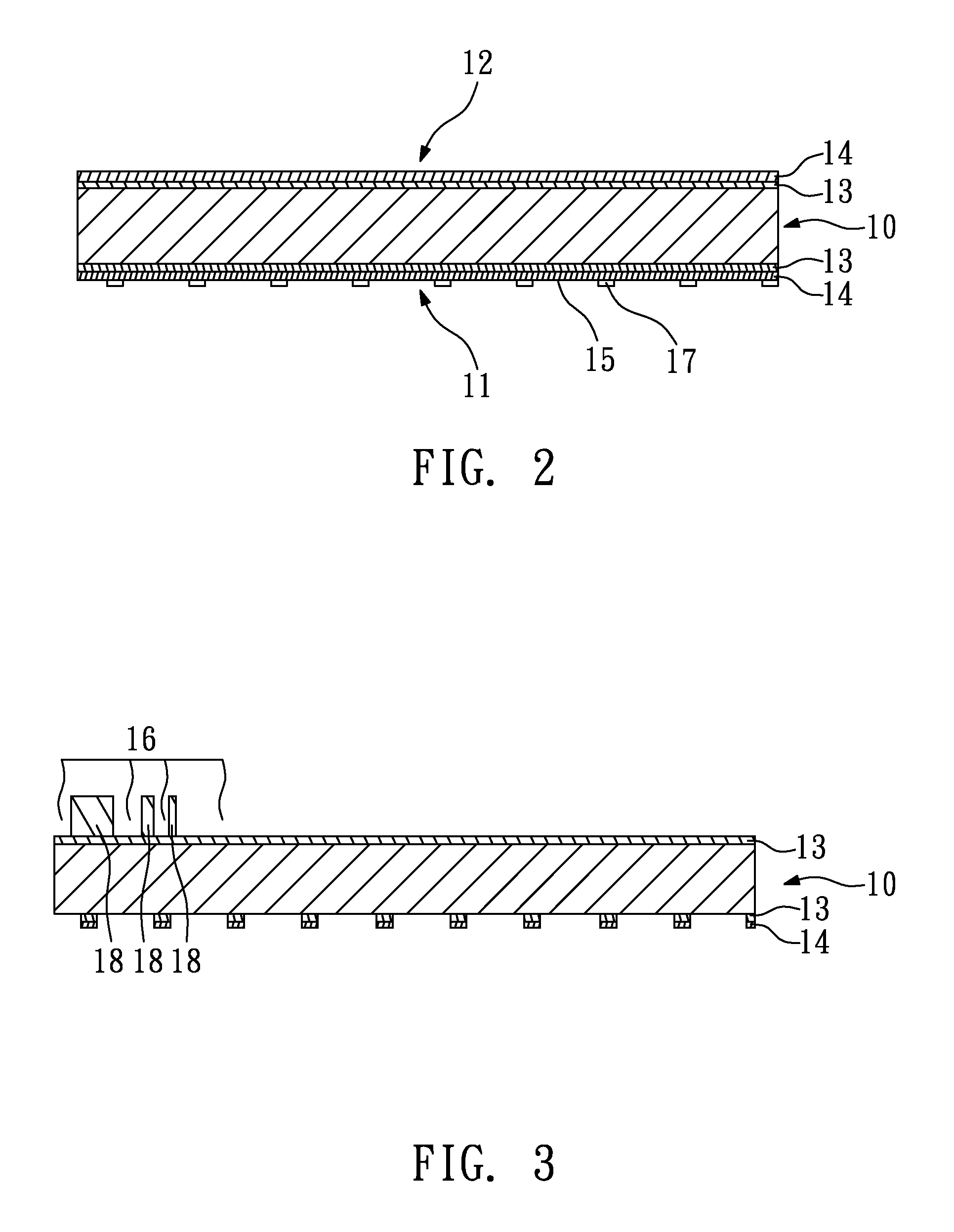
[0016]As shown in FIGS. 2 and 3, a first pattern 15 and a second pattern 16 are defined on the first side surface 11 and the second side surface 12, respectively. In this embodiment, a first photoresist mask 17 is used on the first side surface 11 to define the first pattern 1...


PUM


Abstract

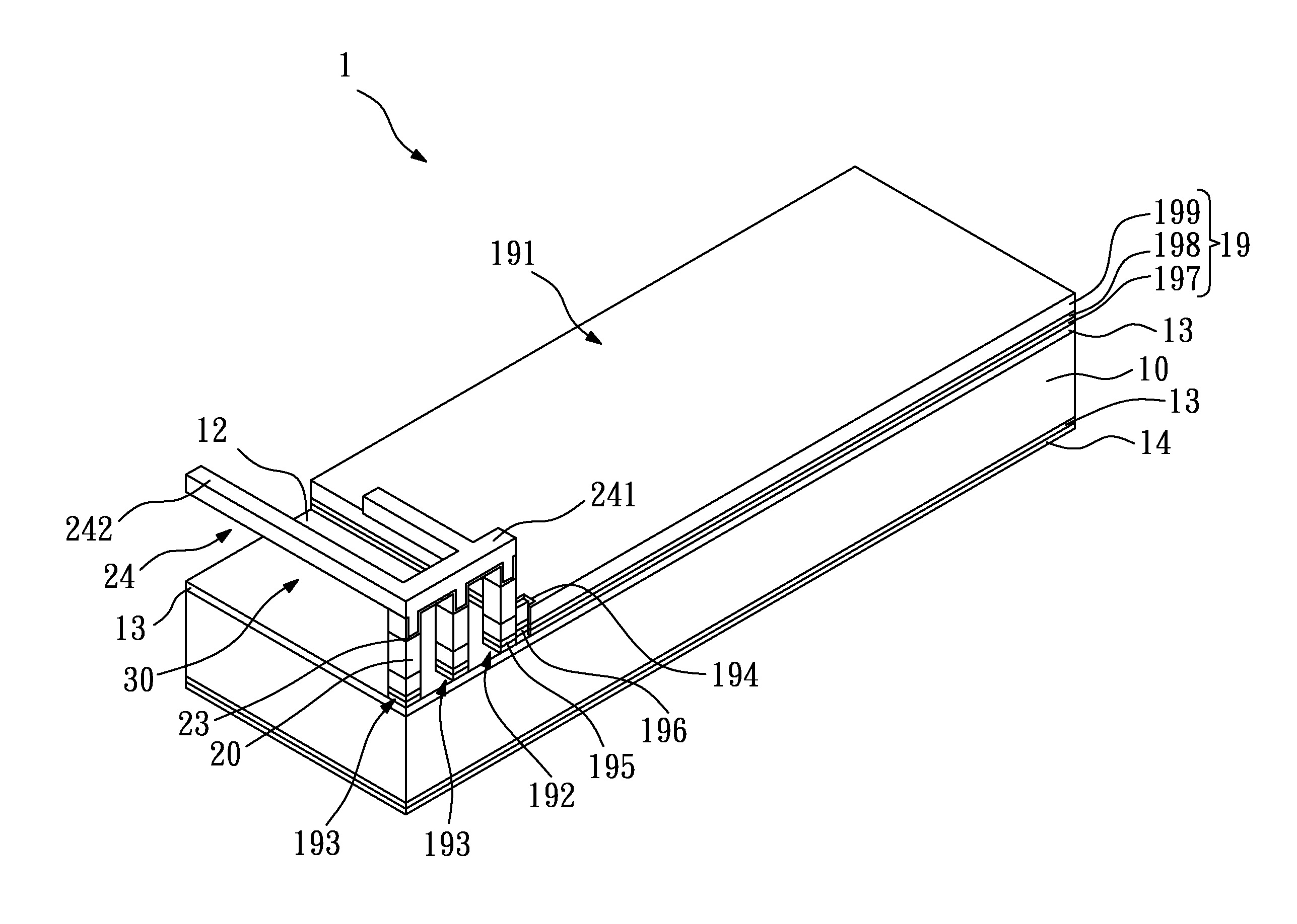
The disclosure provides a silicon-based suspending antenna with photonic bandgap structure which manufactured by IC thin film process, surface micromachining and bulk Micromachining are provided. The silicon-based suspending antenna with photonic bandgap structure includes a silicon substrate, an electrode layer, a spacing part and an F-shaped structure. The silicon substrate has a first side surface and a second side surface oppositing to the first surface, the first side surface has a plurality of regular recesses and the second side surface has a longitudinal edge. The electrode layer has a flat part, a first base and at least one second base, in which one side of the flat part has a notch, the first base, the second base and the notch are separately disposed on the second side surface and essentially parallel to the longitudinal edge of the second side surface, the first base has a main body and an extension, and the extension extends from the main body and into the notch. The spacing part is disposed on the second base. The F-shaped structure has a longitudinal part disposed on the spacing part and is parallel to the second side surface.

Description

BACKGROUND[0001]1. Technical Field[0002]The disclosure relates to an antenna and method for making the same, and more particularly to a silicon-based suspending antenna with photonic bandgap structure and method for making the same.[0003]2. Description of the Related Art[0004]In ultra-wideband (UWB) technology, bandwidth between 3.1 GHz to 10.6 GHz is often applied to imaging system, automotive radar system, communications and measurement system, as a wireless transmission multimedia interface of short range and high speed, to form an important technique of seamless communication. In recent years, wireless personal network (WPAN) systems have been defined in UWB, mainly for digital data transmission within a range of 10 meters. In addition, UWB has a high bandwidth and high transmission rate (up to a maximum of 500 Mbps), as well as low power consumption, high security, high transmission speed, low interference, precision positioning function, and low-cost chip structure, which make...

Claims


Application Information

Patent Timeline
Patent Type & Authority Applications(United States)
IPC IPC(8): H01Q1/12B05D5/12
CPCH01Q1/38H01Q15/006H01Q5/364H01Q5/0055H01Q5/25H01Q5/0017
Inventor HUANG, I-YUSUN, CHIAN-HAOHSU, KUO-YI
Owner IND TECH RES INST
Learn More