Luminescent optical device and solar cell system with such luminescent optical device

a luminescent optical and solar cell technology, applied in the direction of instruments, lighting and heating apparatus, planar/plate-like light guides, etc., can solve the problems of high investment cost, high maintenance cost, and high cost of solar energy generation in photovoltaic systems, so as to reduce the size of the light receiving surface and reduce the cost of the photovoltaic cell. , the effect of efficient emission of ligh

Active Publication Date: 2012-05-17
MERCK PATENT GMBH
View PDF5 Cites 41 Cited by
  • Summary
  • Abstract
  • Description
  • Claims
  • Application Information

AI Technical Summary

Benefits of technology

[0088]In an embodiment, the optical exit surface and the light receiving surface are in contact with each other. This may advantageously allow an efficient transfer of emission light from the optical device onto the photovoltaic cell.
[0089]In an embodiment, the solar cell system further comprises a light collection waveguide, arranged to receive emission light escaping from the optical waveguide by the optical exit surface, and arranged to transport the emission light as received to the light receiving surface, whereby the light receiving surface is arranged to receive emission light escaping from the optical waveguide by the optical exit

Problems solved by technology

The cost of generating solar energy per unit Watt in a photovoltaic system is several times higher than generating energy from other sources, which include coal, oil, wind, biomass and nuclear energy.
These devices have several disadvantages, including high investment cost, high maintenance cost, unwieldy shapes, and the necessity of tracking the sun as it crosses the sky, requiring mechanical constructions to physically alter the orientation of the device, the mirrors, lenses and/or the photovoltaic cell (PV cell).
This not only increases efficiency, but also decreases cost, as luminescent solar concentrator panels can be made cheaply from plastics, while PV-cells need to be completely constructed from expensive materials such as purified silicon.
At the moment, LSC-systems are not used commercially which is predominantly related to their relatively poor efficiency.
This low overall efficiency originates from a high re-absorption of emi

Method used


Image

  • Luminescent optical device and solar cell system with such luminescent optical device
  • Luminescent optical device and solar cell system with such luminescent optical device
  • Luminescent optical device and solar cell system with such luminescent optical device

Examples


first embodiment

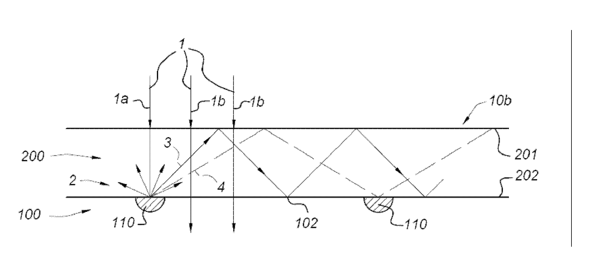
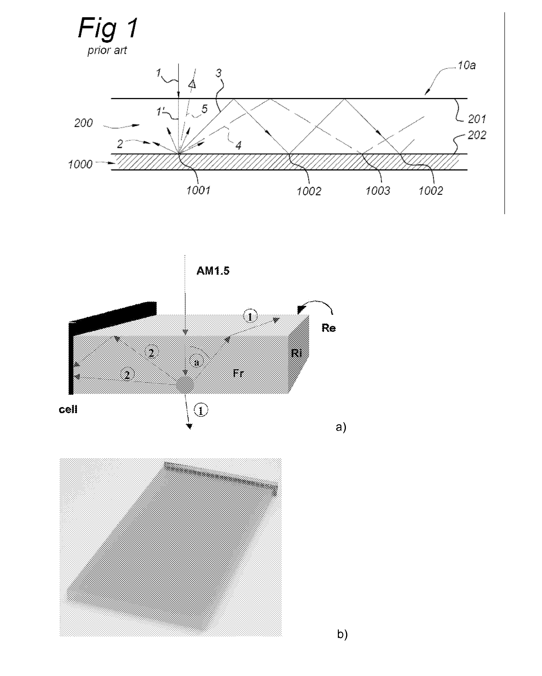
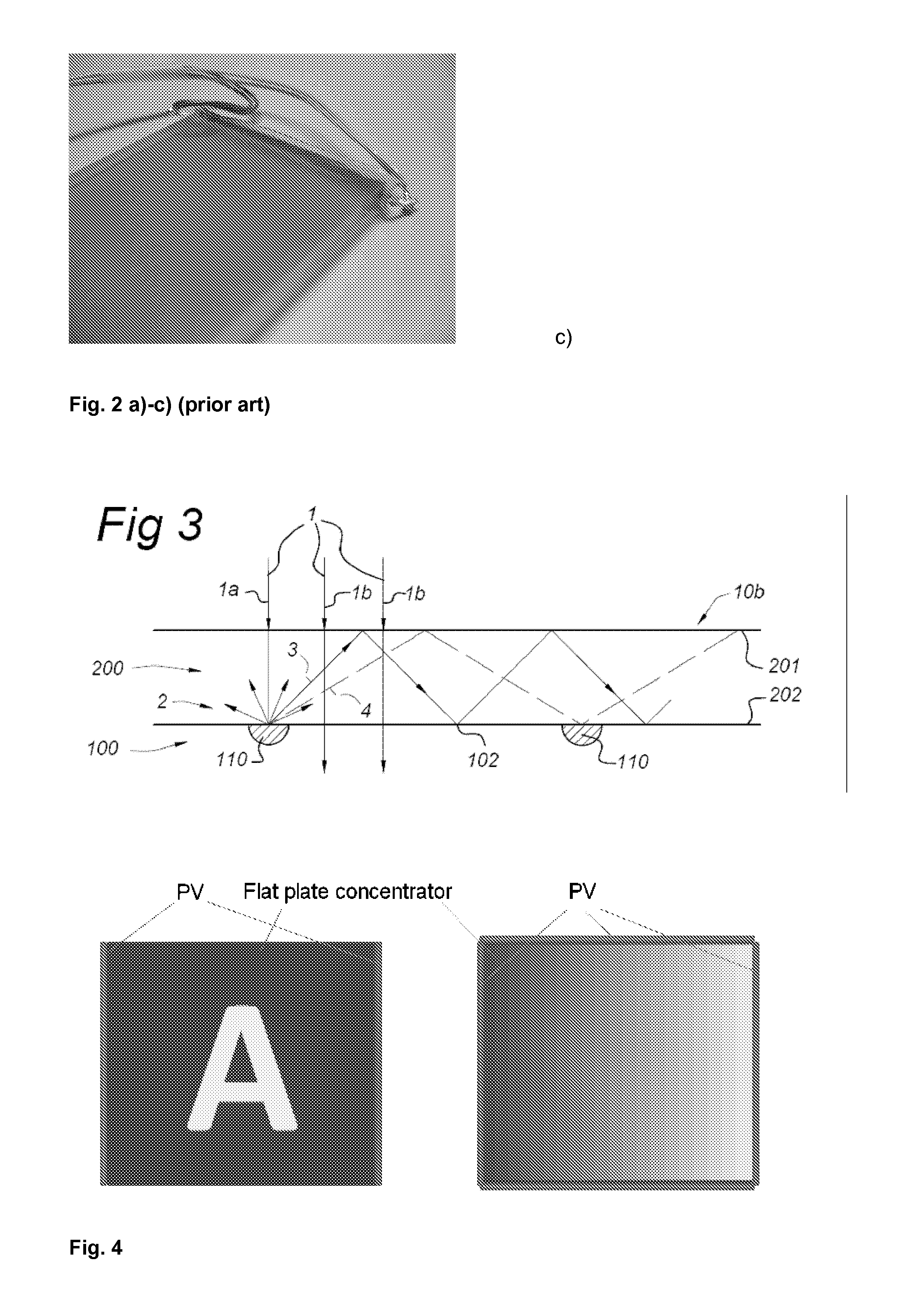
[0147]FIG. 17 schematically shows a luminescent optical device 10 according to the invention according to a The lens structure 300 has a plurality of lenses 310, which extend along a long axis perpendicular to a short axis, the lenses 310 have a generally line-shaped focus on respective line-shaped luminescent domains 110 extending parallel to the ling axis of the respective lens 310. These lenses may further be referred to as cylindrical lenses 310L. The cylindrical lenses 310L are arranged side-by-side in a one-dimensional array. Each cylindrical lens has an aspherical cross section over the short axis of the lens 310L. The cross section is substantially constant over the long axis of the lenses 310L. The luminescent optical device 10 is preferably oriented during use with the long axis of the cylindrical lenses 310L arranged substantially east-west, and its short axis north-south, thereby focusing sun light onto the luminescent domains 310 over a large section of the sun's altit...

second embodiment

[0148]FIG. 18 schematically shows a luminescent optical device 10 according to the invention according to a The lens structure 300 has a plurality of lenses 310, which have a substantially circular shape (when observed in a top view), the lenses 310 have a generally dot-shaped focus on respective dot-shaped luminescent domains 110. These lenses may further be referred to as circular lenses 310C. The circular lenses 310C are arranged side-by-side in a two-dimensional array. In the example shown, the two-dimensional array is a square grid, but the two-dimensional array may alternatively be e.g. a hexagonal array wherein the circular lenses 310C are arranged in a closed-packed arrangement. The luminescent domains 310 are arranged in a corresponding two-dimensional array. Each circular lens 310C has an aspherical cross section over its diameter in any direction, which is designed to provide a large angular acceptance range over a large section of the sun's altitude trajectory. The angu...


PUM

PropertyMeasurementUnit
Fractionaaaaaaaaaa
Angleaaaaaaaaaa
Fractionaaaaaaaaaa

Abstract

The invention provides a luminescent optical device (10) having an optical waveguide (200). The luminescent optical device (10) further has a photo-luminescent structure (100) on or inside the optical waveguide (200). The photo-luminescent structure (100) comprises a plurality of photo-luminescent domains (110) containing photo-luminescent material (120). The photo-luminescent material (120) is capable of emitting emission light upon excitation by excitation light. The photo-luminescent domains (110) are arranged to emit, upon excitation by excitation light, at least part of the emission light into the optical waveguide layer (200). The luminescent optical device (10) further may comprise a lens structure (300) on the optical waveguide (200). The lens structure (300) comprises a plurality of lenses (310), arranged to capture incident light provided from an external light source, in particular the sun, and to concentrate the incident light onto the plurality of photo-luminescent domains (110) as excitation light for excitation of the photo-luminescent material (120).

Description

FIELD OF THE INVENTION[0001]The invention relates to a luminescent optical device, more particularly to a luminescent solar concentrator (LSC), and a solar cell system with such luminescent optical device.BACKGROUND OF THE INVENTION[0002]The cost of generating solar energy per unit Watt in a photovoltaic system is several times higher than generating energy from other sources, which include coal, oil, wind, biomass and nuclear energy. In order to reduce the cost of solar energy generation in photovoltaic systems, it is desirable to make efficient use of the most expensive part of the system, namely the photovoltaic cell (herein also referred to as the solar cell). Conventionally, this is done by using large light-focusing parabolic mirrors or large Fresnel lenses, with the photovoltaic cell positioned in the focal point of the parabolic mirror or Fresnel lens. These devices have several disadvantages, including high investment cost, high maintenance cost, unwieldy shapes, and the ne...

Claims


Application Information

Patent Timeline
IPC IPC(8): H01L31/0232F21V5/04B32B37/16F21V8/00
CPCG02B6/004G02B6/0053G02B6/0058H01L31/0547Y02E10/52H01L31/0522H01L31/0543H01L31/055H01L31/054
Inventor DEBIJE, MICHAEL GEORGEVAN OOSTEN, CASPER LAURENSBASTIAANSEN, CORNELIS WILHELMUS MARIATSOI, SHUFEN
Owner MERCK PATENT GMBH
Why Eureka
Try Eureka