Semiconductor device with lateral element

a technology of lateral element and semiconductor device, which is applied in the direction of semiconductor device, basic electric element, electrical apparatus, etc., can solve the problems of reducing the resistance value of transitional withstanding voltage, increasing the switching loss and occurrence of damage to the element, and difficult to meet the requirements of micro inverter such as high speed operation, high efficiency and low loss, so as to reduce the resistance value and reduce the damage to the lateral element. , the effect of switching loss of the lateral elemen

Inactive Publication Date: 2012-05-17
DENSO CORP
View PDF4 Cites 14 Cited by
  • Summary
  • Abstract
  • Description
  • Claims
  • Application Information

AI Technical Summary

Benefits of technology

[0008]The present invention is made in view of the aforementioned matter, and it is an object to provide a semiconductor device having a lateral element that is capable of restricting the avalanche breakdown and reducing the switching loss and damage to the element, even in a high speed switching operation.
[0010]In such a configuration, since the resistance value of the total resistance of the SRFP is set in the range between 90 kΩ and 90 MΩ, it is less likely that the amount of decrease in an electric current at a second peak of peaks where the amount of electric current largely reduces at a time of turning on will be increased. Therefore, even if the semiconductor device is operated at high speed, avalanche breakdown is restricted, and switching loss of the lateral element and damage to the lateral element can be reduced.
[0011]For example, when the insulation film has a thickness of 200 nm to 1000 nm, the above described advantageous effect is achieved.
[0015]The electric field concentration at the SRFP adjacent to the second electrode is caused because it is difficult to follow a change in voltage at a time of switching at a position away from the changing point due to a time constant, though the portion adjacent to the changing point can immediately follow the change in voltage. Therefore, by reducing the resistance value per unit length toward the second electrode, the portion away from the changing point can follow the change in voltage at the time of switching. As such, the avalanche breakdown is restricted, and the switching loss of the lateral element and the damage to the lateral element can be reduced.

Problems solved by technology

However, when the lateral power element employing the SRFP is switched at high speed, the electric field reduction by the SRFP will be uneven, resulting in avalanche breakdown and a decrease in transitional withstanding voltage.
Thus, there are possibilities of an increase in switching loss and an occurrence of damage to the element.
As such, if a micro inverter is made using a lateral power element in which the SRFP having the structure described in the documents 1, 2 or the like is employed, it will be difficult to satisfy requirements of the micro inverter such as high speed operation, high efficiency and low loss.

Method used


Image

  • Semiconductor device with lateral element
  • Semiconductor device with lateral element
  • Semiconductor device with lateral element

Examples


first embodiment

[0042]A first embodiment of the present invention will be described. In the present embodiment, an inverter for driving a three-phase motor will be described as an example of a semiconductor device having a lateral element.

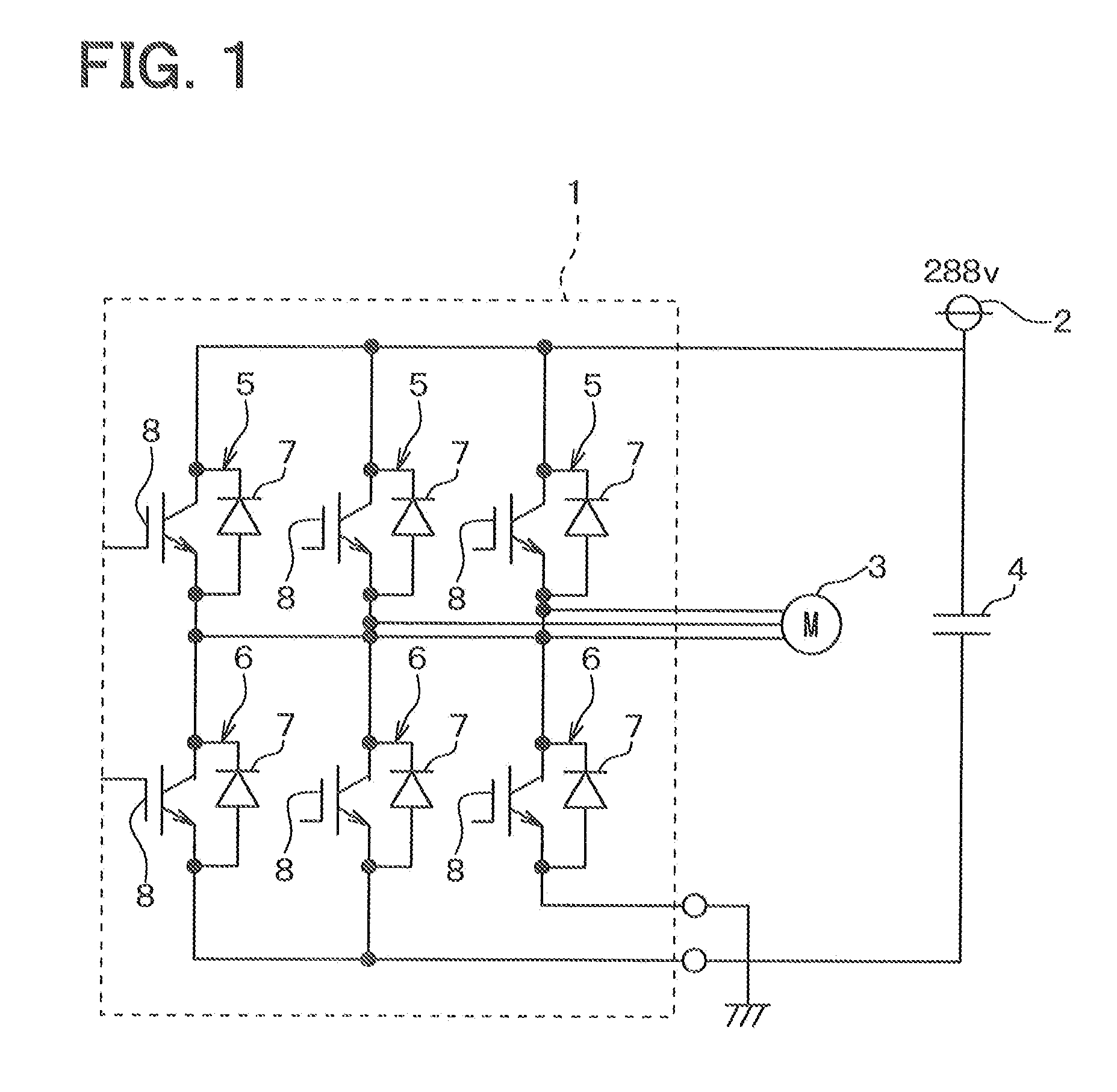
[0043]FIG. 1 is a circuit diagram of an inverter 1. As shown in FIG. 1, the inverter 1 is used to alternating-current drive a three-phase motor 3 as a load based on a direct-current power source 2.

[0044]The inverter 1 includes three series sections, each having an upper arm 5 and a lower arm 6 connected in series, corresponding to the three phases of the motor 3, and the three series sections are connected in parallel to each other. The inverter 1 successively applies the middle potential between the upper arm 5 and the lower arm 6 of each series section to corresponding one of a U-phase, a V-phase and a W-phase of the three-phase motor 3. Each of the upper arm 5 and the lower arm 6 has a lateral FWD 7 and a lateral IGBT 8. As the IGBTs 8 of the upper and lower ar...

second embodiment

[0110]A second embodiment of the present invention will be described hereinafter. In the present embodiment, the structure of the SRFP 21, 34 is modified from that of the first embodiment, and other structures are similar to the first embodiment. Thus, a part different from the first embodiment will be mainly described.

[0111]In the first embodiment, the resistance value of the total resistance R of the SRFP 21, 34 of the lateral element such as the lateral FWD 7 and the lateral IGBT 8 is adjusted. In such a case, it is assumed that the resistance value of the SRFP 21, 34 is constant in the longitudinal direction. Alternatively, the resistance value of the SRFP 21, 34 is not limited to be constant in the longitudinal direction, but may be varied in the longitudinal direction.

[0112]FIG. 18 is an enlarged view of a part of the SRFP 21, 34 of the lateral FWD 7 and the lateral IGBT 8 when viewed from the top, As shown in FIG. 18, the SRFP 21, 34 has portions that provides regions R1, R2 ...

third embodiment

[0116]A third embodiment of the present invention will be described. The present embodiment employs a semiconductor substrate other than the 301 substrate 1 of the first embodiment, and structures of the present embodiment other than the semiconductor substrate are similar to those of the first embodiment. Therefore, a different structure will be mainly described.

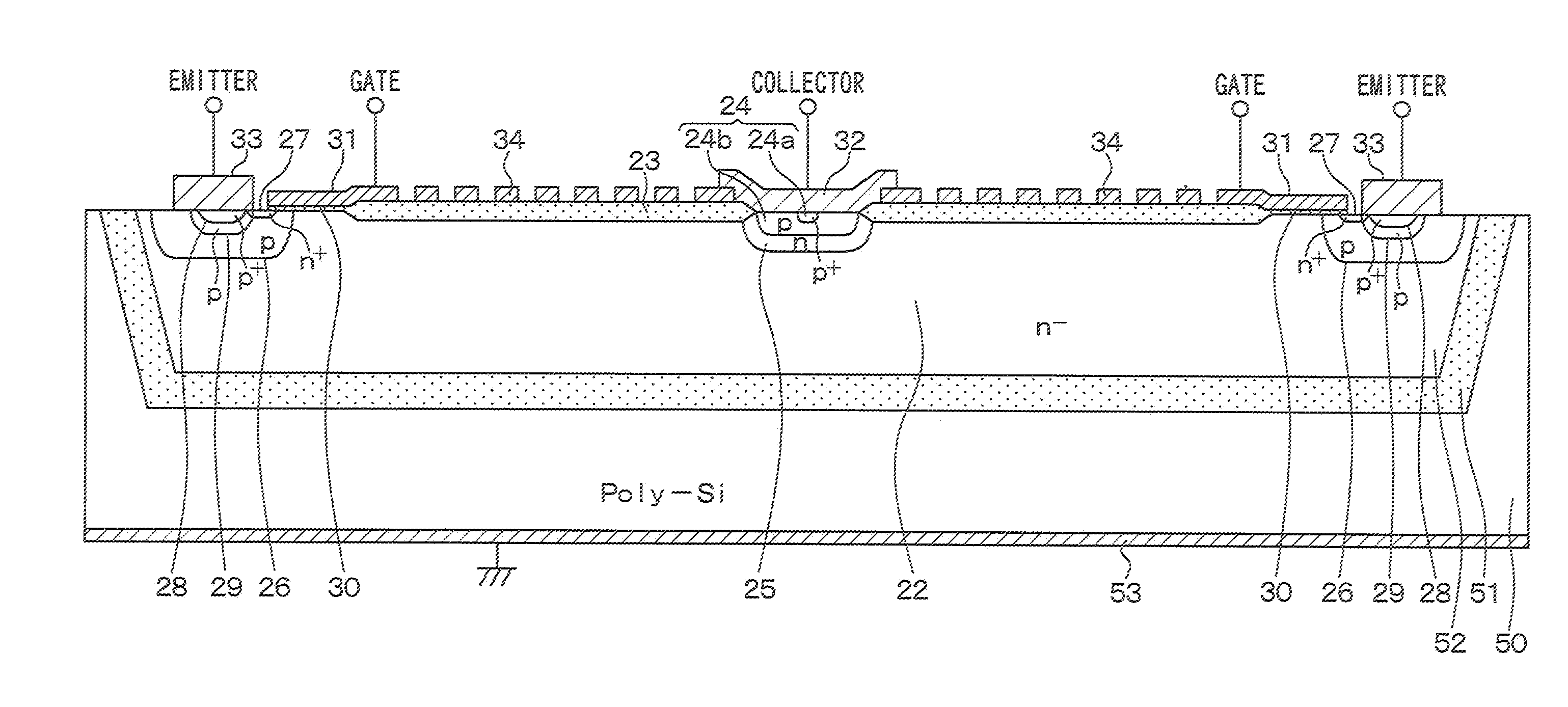
[0117]FIG. 19 is a diagram illustrating a cross-sectional structure of the n-channel lateral IGBT 8 according to the present embodiment. As shown in FIG. 19, a semiconductor substrate 40 in which an n−-type layer 42 is formed on a p−-type silicon substrate 41 is used. Further, the n−-type drift layer 22 is provided by the n−-type layer 42, and a p+-type isolation region 43 is formed to extend from the surface of the n−-type drift layer 22 to the p−-type silicon substrate 41.

[0118]The p+-type isolation region 43 is formed to surround the periphery of the lateral IGBT 8, and a junction isolation structure is provided by PN ju...


PUM


Abstract

In a semiconductor device in which a first electrode and a second electrode are disposed on a surface of a first conductivity-type semiconductor layer of a semiconductor substrate and a lateral element is formed to cause an electric current between the first electrode and the second electrode, a scroll-shaped resistive field plate is disposed on the semiconductor layer across an insulation film. The resistive field plate extends toward the second electrode while surrounding a periphery of the first electrode in a scroll shape. A resistance value of a total resistance of the resistive field plate is in a range between 90 kΩ and 90 MΩ.

Description

CROSS REFERENCE TO RELATED APPLICATION[0001]This application is based on Japanese Patent Applications No. 2010-255030 filed on Nov. 15, 2010 and No. 2011-246104 filed on Nov. 10, 2011, the disclosure of which are incorporated herein by reference.FIELD OF THE INVENTION[0002]The present invention relates to a semiconductor device having a lateral element such as a lateral diode and a lateral insulated gate bipolar transistor (hereinafter referred to as the lateral IGBT), and is, for example, suitably used to a semiconductor device having a lateral diode or a lateral IGBT formed in a SOI (Silicon on insulator) substrate.BACKGROUND OF THE INVENTION[0003]Conventionally, there has been a scroll-shaped resistive field plate (hereinafter referred to as the SRFP (Scroll-shaped Field Plate)) as an electric field reduction technology (see, for example, documents 1 and 2). The SRFP has been used in high voltage lateral diode, lateral IGBT, and lateral power MOSFET. It is appreciated that the SR...

Claims


Application Information

Patent Timeline
Patent Type & Authority Applications(United States)
IPC IPC(8): H01L29/06
CPCH01L29/0696H01L29/404H01L29/8611H01L29/7394H01L29/861H01L29/735
Inventor TOKURA, NORIHITOYAMAMOTO, TAKAOKATO, HISATOSENDA, KOUJINAKAGAWA, AKIO
Owner DENSO CORP
Why Eureka
Try Eureka