

Adder
- Summary
- Abstract
- Description
- Claims
- Application Information
AI Technical Summary
Problems solved by technology
Method used
Image


Examples
first embodiment
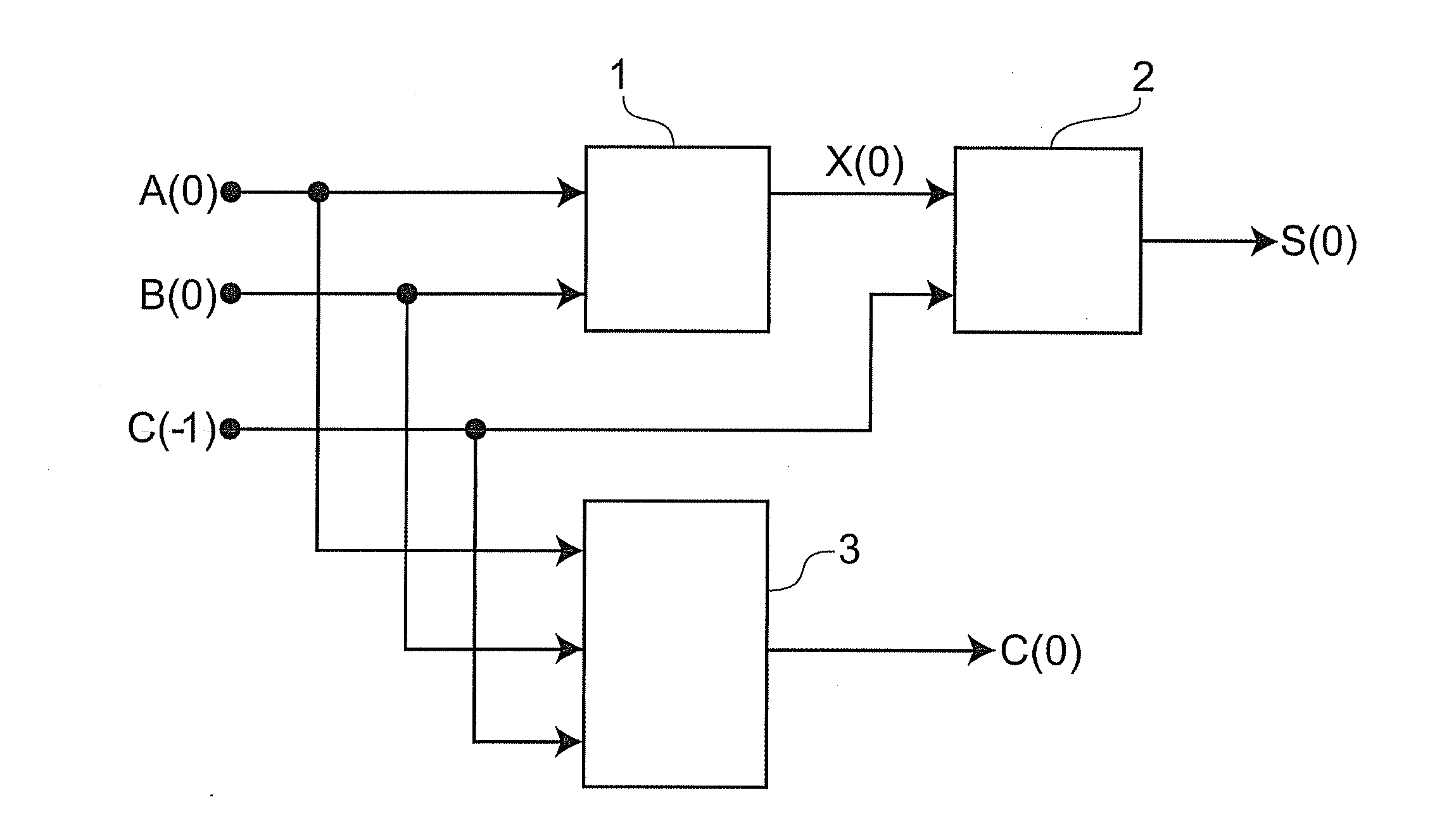
[0041]FIG. 1 is a block diagram schematically showing the configuration of a 1-bit adder according to a first embodiment. In particular, FIG. 1 corresponds to the case of m=1, k=1. A(0) and B(0) are signals corresponding to the bit value A[i] and the bit value B[i] of the i-th position of n-bit (n is an integer of 1 or more) binary values A and B. C(−1) is the carry signal from a less significant position corresponding to the carry bit value C[i−1] from the (i−1)-th position to the i-th position. These are all given as electrical signals for one of the inputs represented by “0” corresponding to the bit value 0 or “1” corresponding to the bit value 1. Here, i is one of the integers 0 to n−1. For i equal to 0, C(−1) is an electrical signal corresponding to “0”.
[0042]The computing units 1, 2, and 3 shown in FIG. 1 are multi-input logic units. The computing unit 1 is the first wave computing unit. In response to input of A(0) and B(0), the computing unit 1 outputs an intermediate output...
second embodiment
[0139]FIG. 24 is a block diagram showing an adder according to a second embodiment. The adder according to the embodiment is an (m+1)-bit adder 40. In response to input of signals corresponding to signals A(0) to A(m), signals B(0) to B(m), and a signal C(−1), the adder outputs computation results S(0) to S(m), and C(m). The signals A(0) to A(m) correspond to the bit values of the i-th to (i+m)-th positions of a binary value A. The signals B(0) to B(m) correspond to the bit values of the i-th to (i+m)-th positions of a binary value B. The signal C(−1) corresponds to the carry bit value from the (i−1)-th position to the i-th position for the sum of the binary value A and the binary value B. Here, m is an integer of 0 or more.
[0140]A(0) to A(m), B(0) to B(m), and C(−1) are one of the two inputs represented by “0” or “1”. The input terminal of the adder receives input of an electrical signal corresponding to “0” or “1”. On the other hand, the output terminal outputs a signal correspond...
third embodiment
[0154]FIG. 27 is a block diagram showing an m-bit adder 44 according to a third embodiment. The adder 44 according to this embodiment includes q sub-adders (q is an integer of 1 or more). For instance, FIG. 27 shows an example for q=2, including a sub-adder 45 and a sub-adder 46.
[0155]The sub-adder according to this embodiment includes first to n-th addition computing units and a carry computing unit. In response to input of signals corresponding to the bit values A[j] to A[j+n−1] and B[j] to B[j+n−1] of the j-th to (j+n−1)-th positions of binary values A and B, and a carry bit value C[j−1], the first to n-th addition computing units output computation results S(j) to S(j+n−1), and the carry computing unit outputs a computation result C(j+n−1) corresponding to the carry bit value C[j+n−1]. Here, j and n are integers, and i≦j, j+n≦i+m.
[0156]The first addition computing unit inputs signals corresponding to two of A[j], B[j], and C[j−1] to the first wave computing unit and causes it to...
PUM
 Abstract
Description
Claims
Application Information