Vertical cavity surface emitting laser with active carrier confinement

a laser and cavity surface technology, applied in semiconductor lasers, laser details, electrical devices, etc., can solve the problems that the carrier injection of both approaches (oxidation and implantation) is not necessarily adapted to the lateral intensity profile of the optical mode, and achieves improved beam quality, enhanced beam intensity, and improved efficiency

Active Publication Date: 2012-05-24
TRUMPF PHOTONIC COMPONENTS GMBH
View PDF3 Cites 17 Cited by
  • Summary
  • Abstract
  • Description
  • Claims
  • Application Information

AI Technical Summary

Benefits of technology

[0019]On the other hand, it is advantageous to design the phototransistor and arrange its position so that the phototransistor does become locally saturated within an area around the maximum light intensity along the base layer. Suitably, this area should not spread along the whole lateral dimensions of the cavity. For example, the phototransistor can be designed so that it becomes saturated within an area of at most the size defined by the FWHM of the lateral light intensity distribution.
[0020]If the phototransistor is locally saturated, the current through the laser diode is not strictly proportional to the light intensity. Thus, the driving current may not be a reliable parameter to monitor the laser output. However, if the base layer is provided with a terminal contact, the photocurrent generated in the base-collector junction can be measured with a monitor circuit connected to the base layer and the at least one collector layer. For the connection of the circuit to the collector layer, either the first or the second terminal contact for injecting electrical current may be used, depending on which of these contacts is on the same side of the collector layer with respect to the base layer. This configuration has also the advantage that a small current can be injected through these contacts to switch the phototransistor and thereby enabling the injection of carriers through the first and second terminal contacts so as to start the lasing operation.
[0021]Besides the effect of an improved efficiency, the invention has the further benefit that the distributed phototransistor also generally improves the beam quality. This is due to the fact that the phototransistor provides a positive feedback to the lateral intensity distribution so that modes having higher intensity are further enhanced. As well, the current aperture which is often used for carrier confinement in general has a lateral refractive index variation which leads to a lateral guidance of optical modes. This in turn increases the tendency for multimode lasing. As an oxide aperture can be omitted according to the invention, this disadvantage of existing VCSELs is avoided. Thus, a laser device according to the invention is expected to have improved single mode features such as a higher single mode output power and a smaller far field angle. The smaller far field angle particularly results from the lack of a lateral refractive index variation which is otherwise induced by the oxide aperture.
[0022]These advantages similarly apply to a device according to the invention lasing in multimode. For multimode lasing, an improved M2-factor is expected.
[0023]The invention is advantageously applicable for high-power top or bottom emitting VCSELs. As the adaptive current confinement provides an improved mode-selectivity, the invention is further particularly suited to realize single-mode VCSELs. Furthermore, it is possible to provide a simplified self-mixing interference sensor with an inventive VCSEL device. In contrast to known interference sensor devices which employ a monitor photodiode, the self-mixing signal can be easily extracted from the laser voltage. Thus, the VCSEL of this device needs only two terminal contacts for operation and measurement, namely the first and second terminal contacts for carrier injection. Circuitry is provided which measures an alternating portion of the voltage across the first and second terminal contacts. The alternating portion predominantly results from the light intensity dependent conductance of the phototransistor. Thus, the phototransistor can also serve as an amplifying element to amplify variations in laser current and voltage induced by self-mixing interference in the laser cavity. In particular, if the phototransistor is operated in the non-saturated regime, a strong dependence of the laser voltage to the light output occurs.
[0024]According to a further embodiment in addition or as alternative to the above mentioned interference sensor, the distributed phototransistor may also advantageously work as a switch which automatically switches between at least two VCSEL electrically connected in parallel, in particular if one of the VCSELs has a failure. This is due to the fact that the light emission dependent amplification of the phototransistors in the VCSELs results in a highly enhanced conductivity through that VCSEL which starts lasing at first. The conductivity through the other phototransistor remains low, so that the current nearly exclusively flows through that VCSEL which starts lasing first and lasing of the other VCSEL is prohibited due to lack of carriers. If, however, the lasing VCSEL fails, the next VCSEL will start lasing. This automatic switching behavior can be achieved most simply with VCSELs having starter terminal contacts bridging one junction of the phototransistor to effectuate self-starting capability of the VCSELs.

Problems solved by technology

However, the carrier injection for both approaches (oxidation and implantation) is not necessarily adapted to the lateral intensity profile of the optical mode.

Method used


Image

  • Vertical cavity surface emitting laser with active carrier confinement
  • Vertical cavity surface emitting laser with active carrier confinement
  • Vertical cavity surface emitting laser with active carrier confinement

Examples


Embodiment Construction

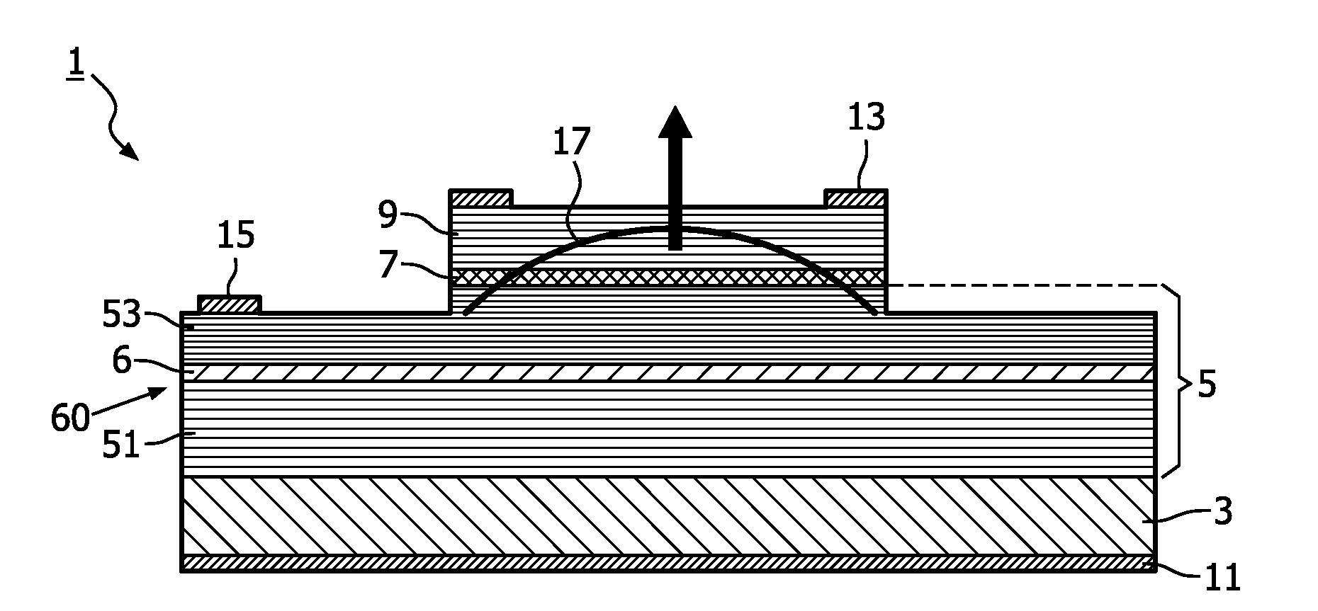
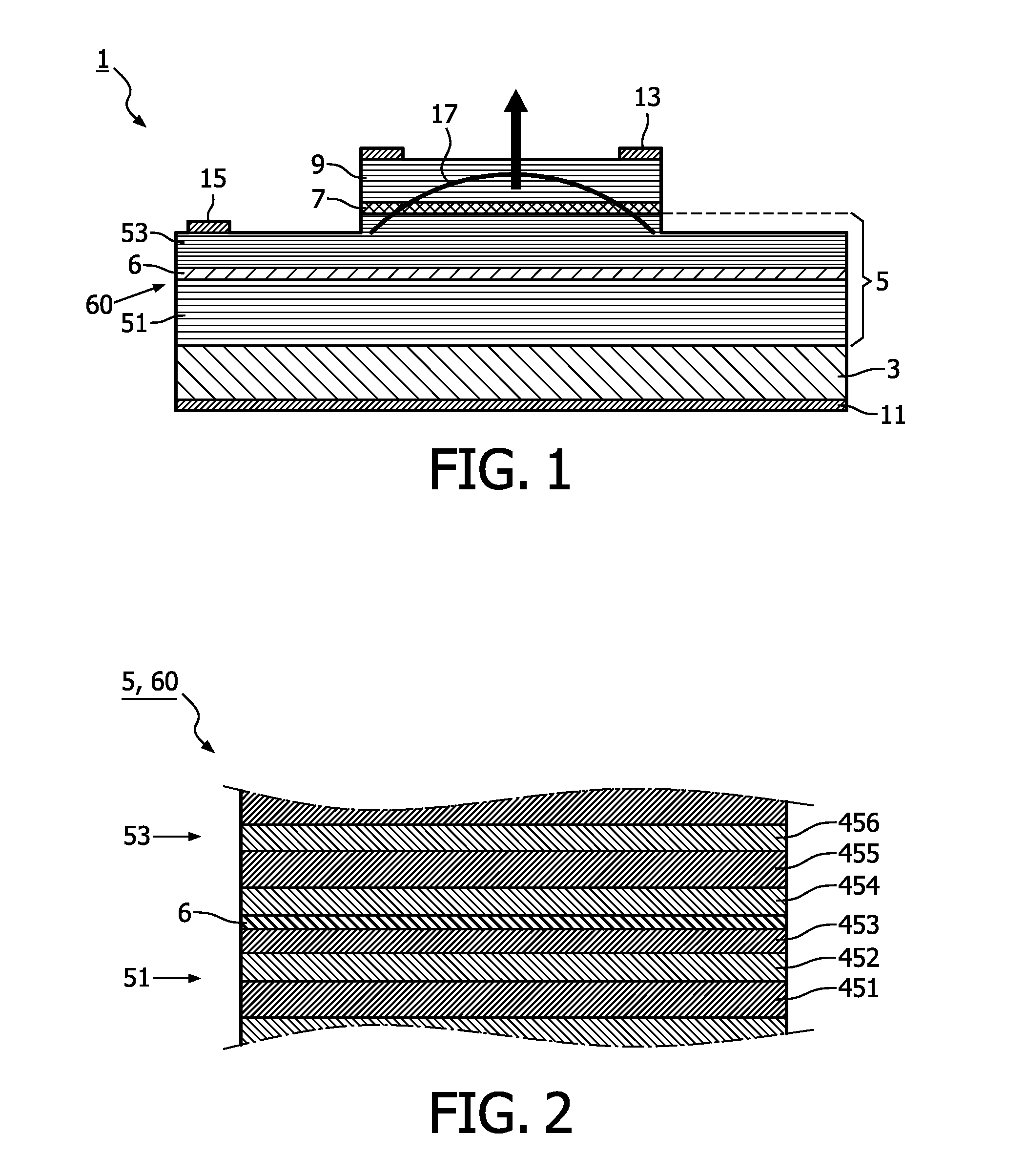
[0033]FIG. 1 shows a schematic of a VCSEL device 1 with an integrated NPN-phototransistor for adaptive carrier confinement. The VCSEL device 1 comprises a substrate 3, and thereon a first layer stack of semiconducting layers which forms a first distributed Bragg reflector 5, an active region 7 with one or more quantum well layers, and a second layer stack of semiconducting layers forming a second distributed Bragg reflector 9.

[0034]A suitable and frequently used material for the substrate is gallium arsenide, GaAs. However, other materials such as indium phosphide (InP) or GaInAsN can be used as well.

[0035]If GaAs is used as the substrate material, the distributed Bragg reflectors 5, 9 can be fabricated by alternating epitaxial growing GaAs and AlGaAs layers. If the substrate is negatively doped, the lower or first distributed Bragg reflector 5 is negatively doped as well, whereas the upper or second distributed Bragg reflector is positively doped. The second distributed Bragg refle...


PUM


Abstract

It is an object of the present invention to improve the confinement of the carriers within a VCSEL. As a general concept of the invention, it is proposed to integrate a phototransistor layer structure into the layer stack of the VCSEL.

Description

FIELD OF THE INVENTION[0001]The invention relates to vertical cavity surface emitting lasers (VCSELs) in general. More specifically, the invention concerns VCSELs having means for current confinement.BACKGROUND OF THE INVENTION[0002]For all semiconductor lasers it is very advantageous to confine the carrier injection as much as possible to the active area that contributes to the lasing activity. Carriers that are injected at spatial positions without overlap with the mode profile are lost. Thus, the better the carrier confinement, the higher is the overall efficiency.[0003]A known measure for confinement of the current close to the center of a VCSEL is an aperture layer having a higher conductivity in the center of the cavity and a lower conductivity at its edge. An aperture layer can be realized by lateral oxidation of a high aluminum containing layer or by local proton implantation. However, the carrier injection for both approaches (oxidation and implantation) is not necessarily ...

Claims


Application Information

Patent Timeline
Patent Type & Authority Applications(United States)
IPC IPC(8): H01S5/187
CPCH01S5/0264H01S5/0601H01S5/0611H01S5/0624H01S2301/18H01S5/0683H01S5/18308H01S5/18347H01S5/423H01S5/0655
Inventor GERLACH, PHILIPP HENNING
Owner TRUMPF PHOTONIC COMPONENTS GMBH
Why Eureka
Try Eureka